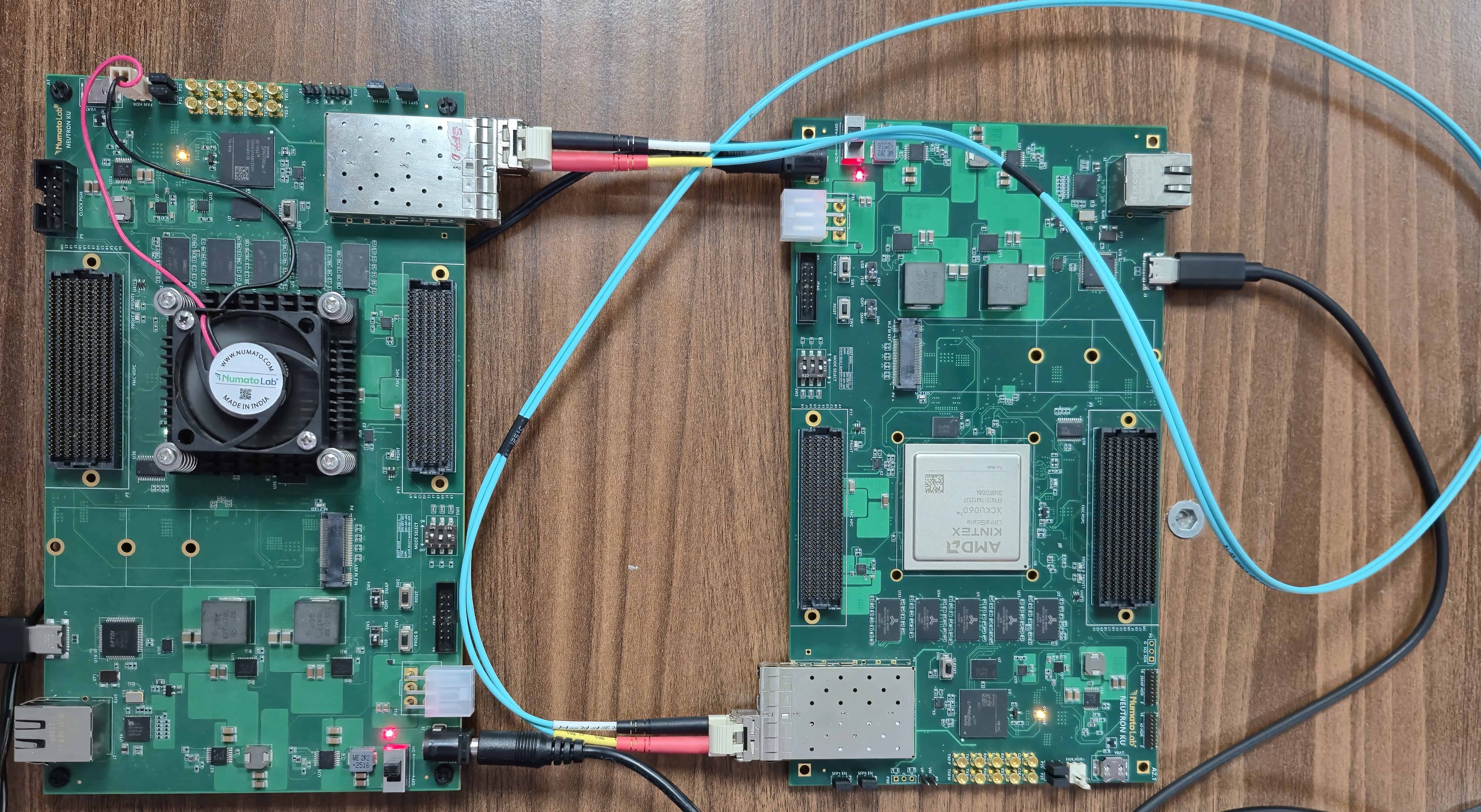
This project demonstrates 1 Gbps Ethernet communication between two Neutron KU60 FPGA Development boards using SFP optical modules. By integrating Vivado-based hardware design, MicroBlaze processing, and Vitis software with the lwIP TCP/IP stack, the system enables reliable bidirectional data exchange over an optical fibre link using the 1000BASE-X standard.
SFP (Small Form-factor Pluggable) modules enable Ethernet communication between devices over optical fibre or compatible copper links. In this project, the FPGA’s Ethernet subsystem processes network data, while the GTH transceiver and SFP module convert it into a high-speed serial signal for transmission to the other Neutron KU60 board. At the receiving end, the SFP module and transceiver recover the data, which is processed by the Ethernet subsystem and delivered to the application using the lwIP TCP/IP stack.
Using 1000BASE-X at 1 Gbps, the two boards can exchange TCP messages over an optical fibre link. This approach provides a practical way to test FPGA-to-FPGA networking, data transfer, and high-speed communication.
The Neutron KU60 FPGA board features two SFP+ cages, enabling high-speed communication with external devices using compatible optical or copper modules. These interfaces are useful for FPGA-to-FPGA networking, high-speed data transfer, and multi-channel communication. In this project, one SFP+ cage on each board is used to establish a 1 Gbps Ethernet link over optical fibre using 1000BASE-X, while the second cage remains available for additional communication experiments.
This guide explains how to establish Ethernet communication between two Neutron KU60 FPGA boards using SFP optical modules. It covers the Vivado hardware design, Vitis software development, lwIP TCP/IP configuration, and UART monitoring through PuTTY. By following these steps, you can implement and test a 1 Gbps point-to-point Ethernet link using 1000BASE-X and exchange messages between the two FPGA boards.
Prerequisites:
- Hardware:
- 2x Neutron KU60 FPGA Development Board
- 2x AMD Platform Cable USB or NLJTPRG002 (Optional)
- 2x USB Type C cable
- 2x 12V DC Power Supply (max 5A current rating)
- 2x SFP optical transceiver modules compatible with the selected 1 Gbps Ethernet mode.
- Duplex LC fibre-optic cable compatible with the SFP modules.
- Software:
- AMD Vivado Design Suite 2024.1
- Vitis Classic 2024.1
- Serial Terminal (PuTTY, Tera Term, etc.)
Let’s get started
Step 1:
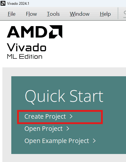
Launch Vivado Design Suite, and go to “File->Project->New” to create a new project. The “New project” wizard will pop up. Click “Next” to continue.
Step 2:
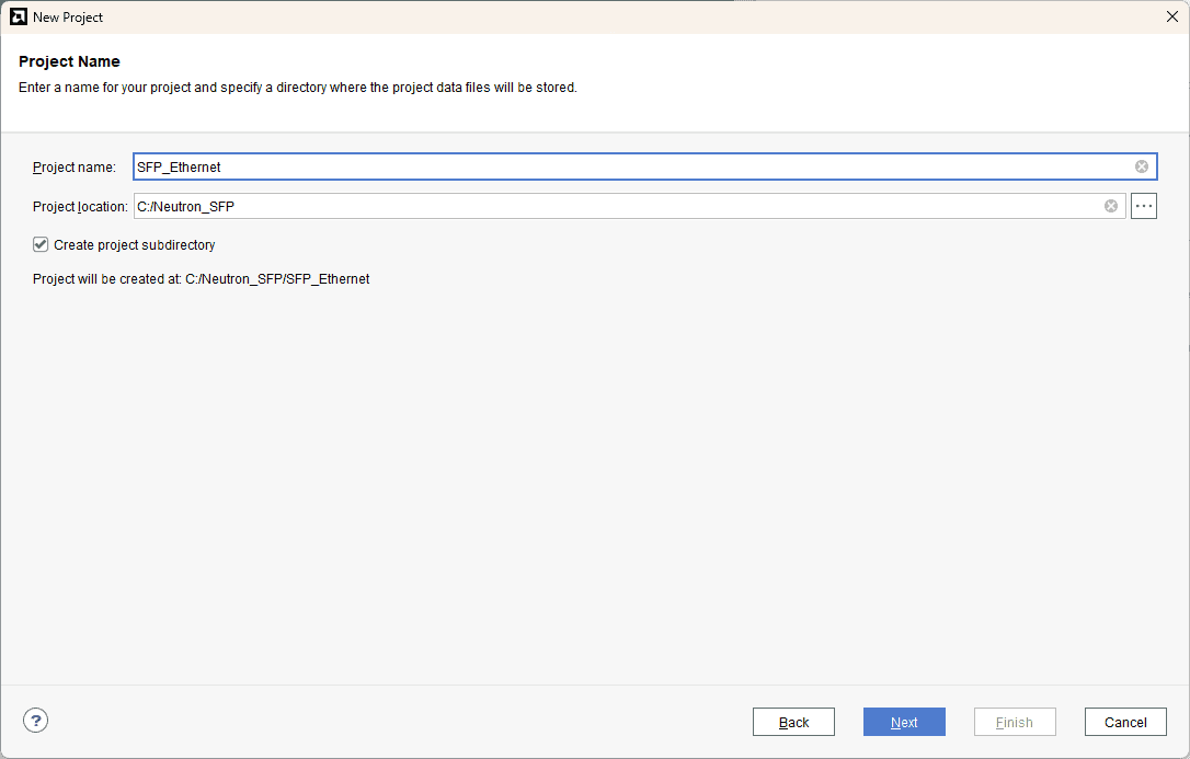
Enter a name for the project and save it at a suitable location. Check the option “Create project subdirectory”. Click Next to continue.
Step 3:
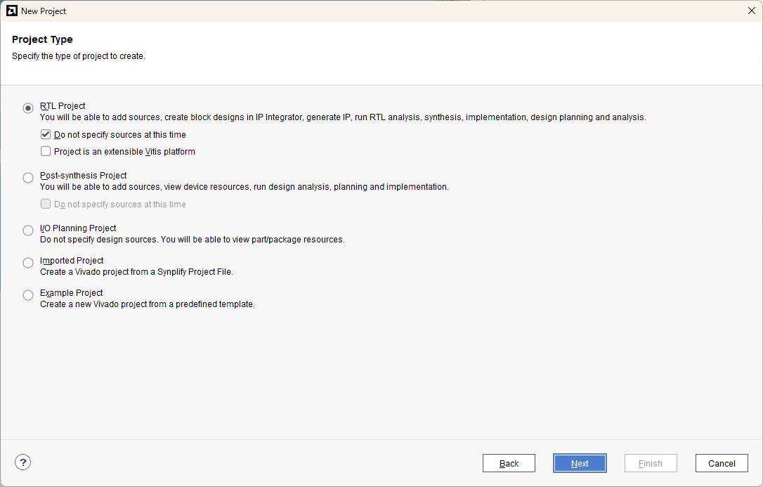
In the “Project type” wizard, select “RTL Project” and select the checkbox to skip specifying the source at the moment. Click “Next“.
Step 4:
At the “Default Part” stage, switch to the “Boards” tab and set the vendor to numato.com. Select “Neutron_KU60” and click Next. If the Neutron_KU60 does not appear in the list, click “Refresh” to update the board catalog. Vivado will then download the latest board files, after which Neutron_KU60 will become available for selection.
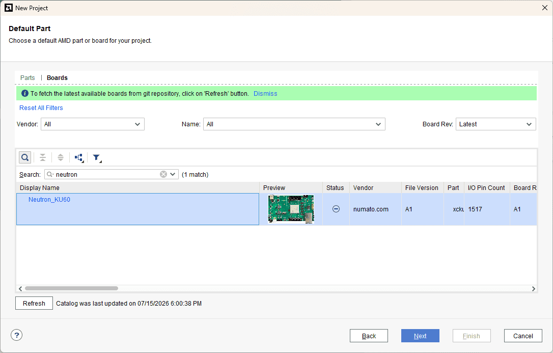
Continue the wizard and finish creating the project. When the new project wizard exits, a new project will be opened up in Vivado with the settings you have selected.
Step 5:
In the Flow Navigator panel, select Create Block Design under IP INTEGRATOR. Enter a name for the block design and click OK. An empty block design will be created
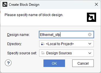
Step 6:
Go to the Diagram window, right-click, and select “Add IP” from the pop-up menu. Search for “MicroBlaze” and add it to the design by double-clicking it.
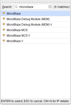
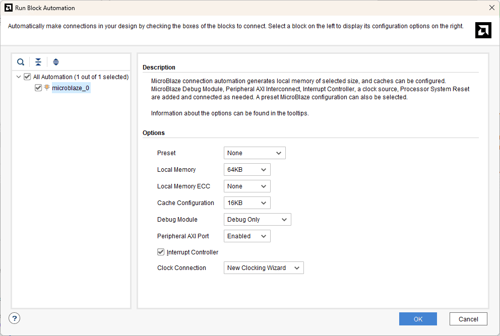
Click “Run Block Automation” present in the “Designer Assistance available” bar on the top left corner of the window to complete the design. Select the settings as shown in the following image. Click “OK” for Vivado to automatically configure the blocks for you.
Step 7:
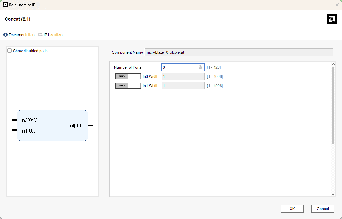
Double click on the Concat ip and configure as per the image below
Step 8:
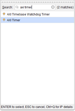
Go to the Diagram window, right-click, and select “Add IP” from the pop-up menu. Search for “AXI Timer” and add it to the design by double-clicking it.
Step 9:
Click the Board tab. The default peripherals available for the Neutron_KU60 board will be displayed.
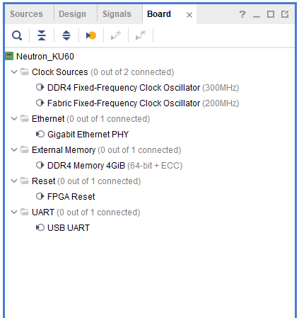
Drag and drop DDR4 Memory 4GiB, USB UART, and Gigabit Ethernet PHY into IP Canvas.
Step 10:
Double click on the ethernet ip AXI 1G/2.5G Ethernet Subsystem to customize it
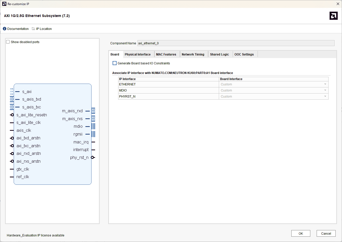
Uncheck the option Generate Board based IO Constraints on the Board tab
Go to the Physical Interface tab and make sure the configuration is as per the below image
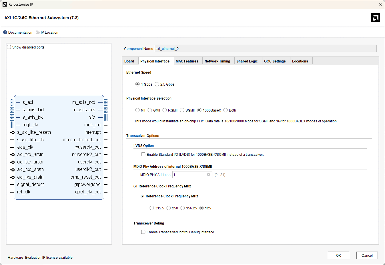
Go to the Locations tab and change the GT location as X0Y18
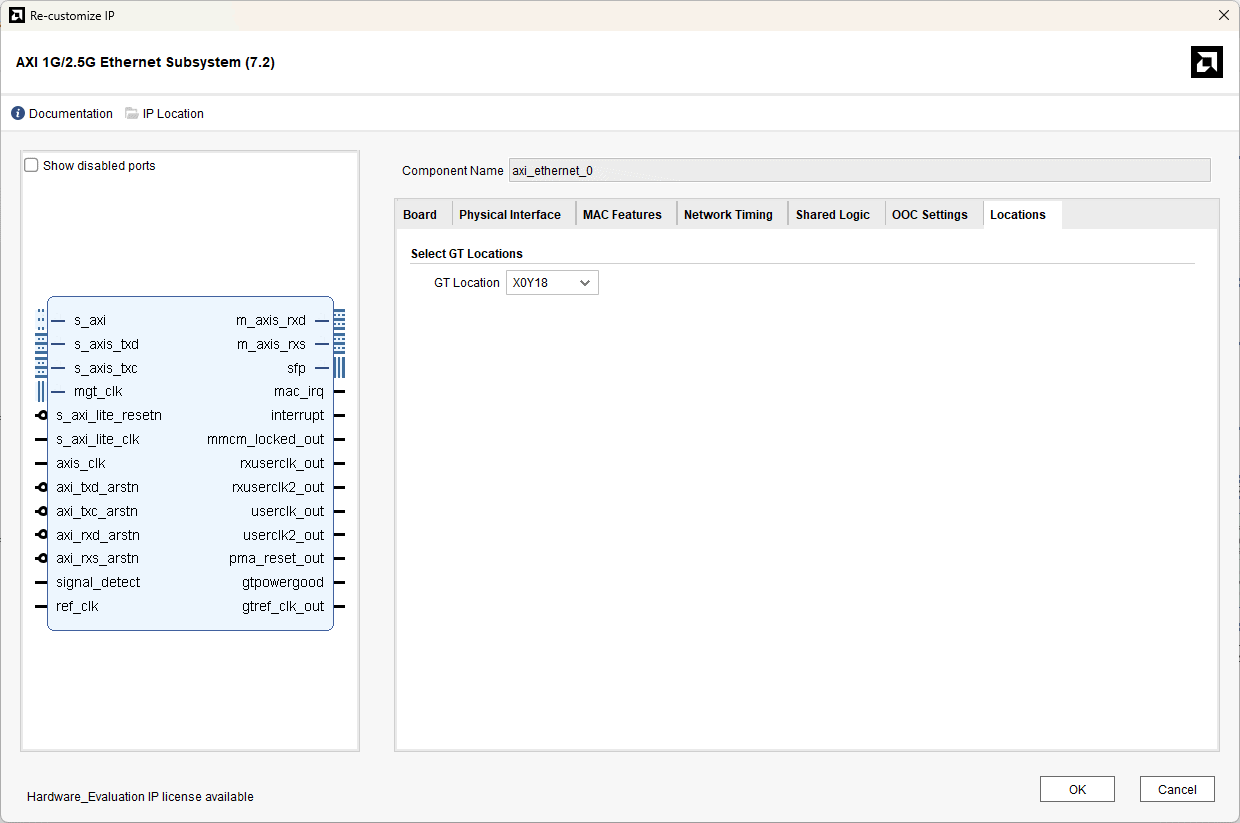
After making these configurations click on OK and the configurations are done.
Step 11:
After configuring the ethernet ip you can see that the ports eth_mdio_mdc , eth_rgmii , phy_reset_out are floating in the design so select them and delete because those ports are for the board preset settings
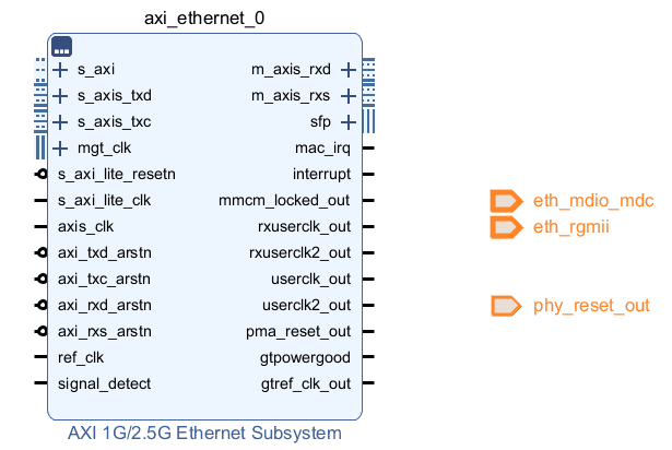
Step 12:
Next you will be able to see a Run Block Automation in the Design Assistance window again , so click on that and run block automation
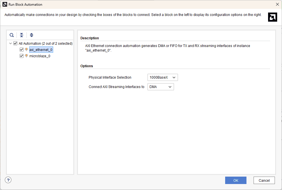
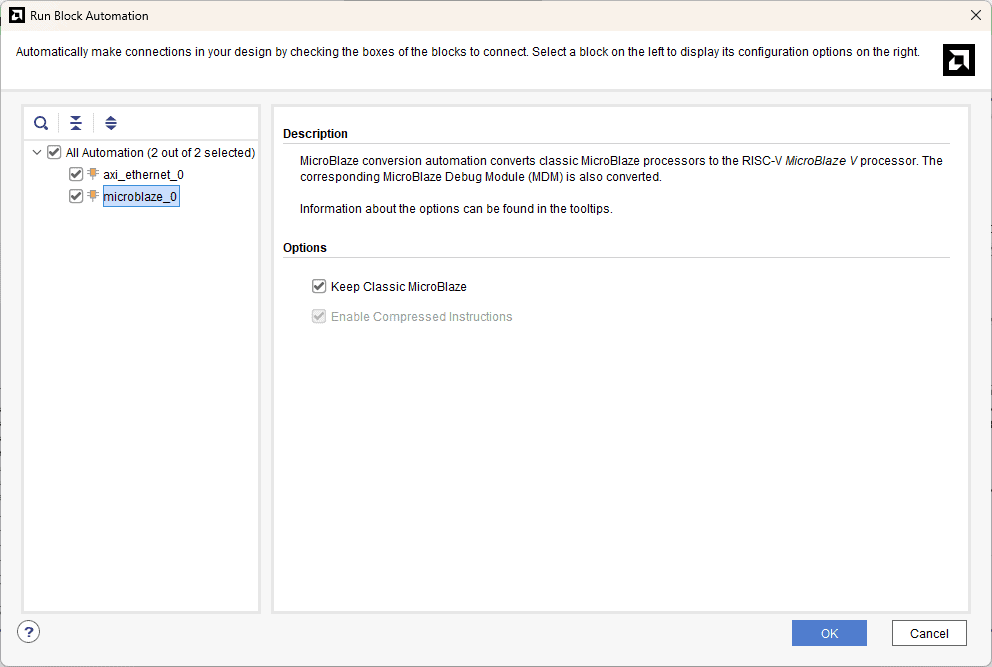
Step 13:
After running the block automation there will be Run Connection Automation option in the Design Assistance window, so run the connection automation now by selecting all
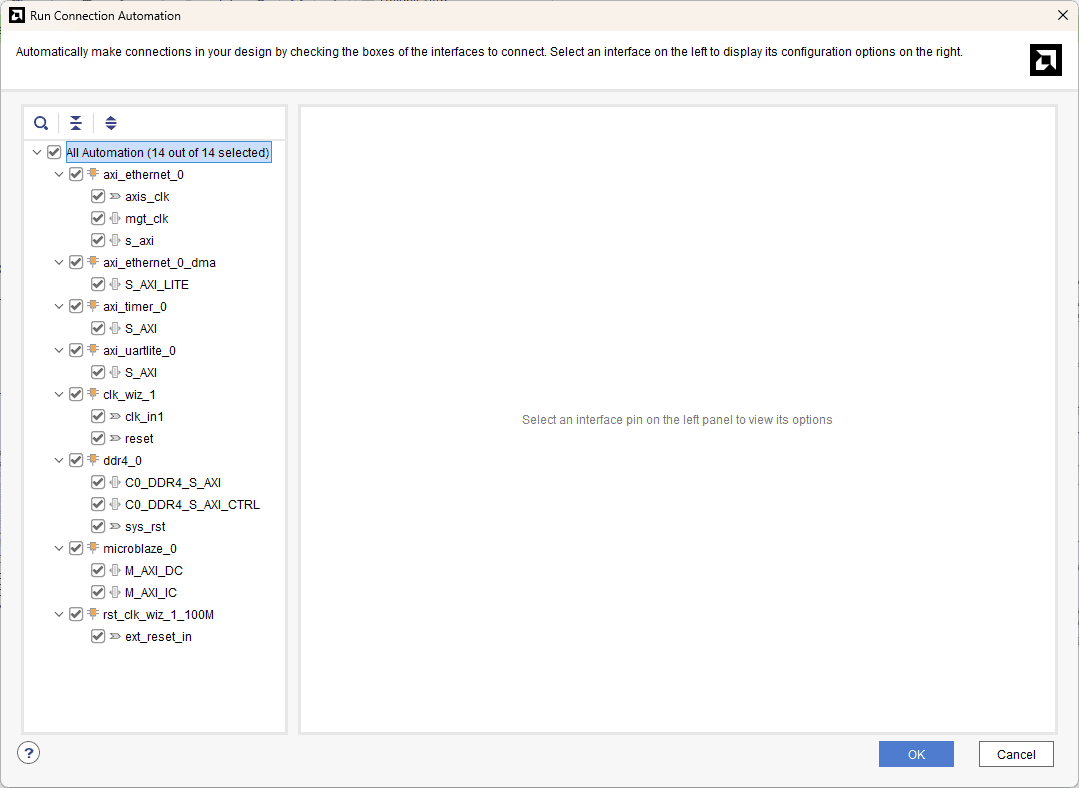
Step 14:
After running connection automation one time , one more option for running connection automation will be available in the design assistance window, run it again.
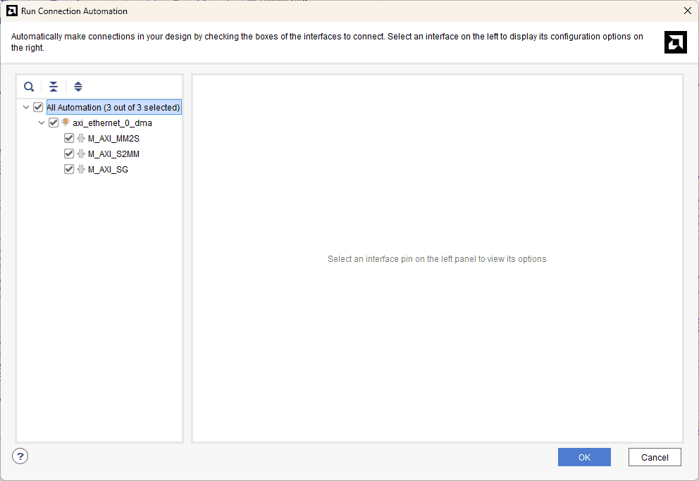
Step 15:
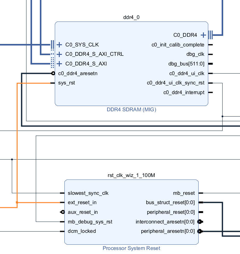
Find the processor system reset block for the clock wizard’s clk_out1 and disconnect its reset pin ext_reset_in
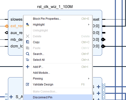
Connect the diconnected reset pin to the sys_rst of the ddr block
Step 16:
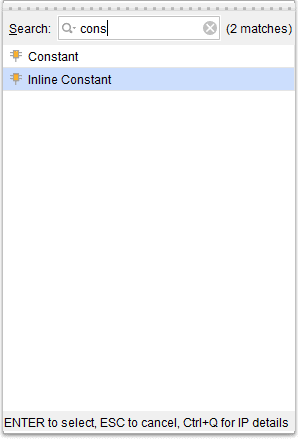
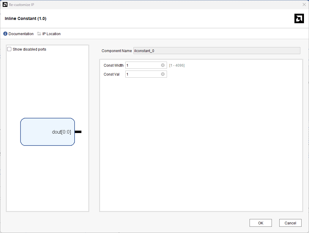
Add a Inline Constant block and set the width and value as 1 and connect to the signal detect pin of the ethernet ip
Step 17:
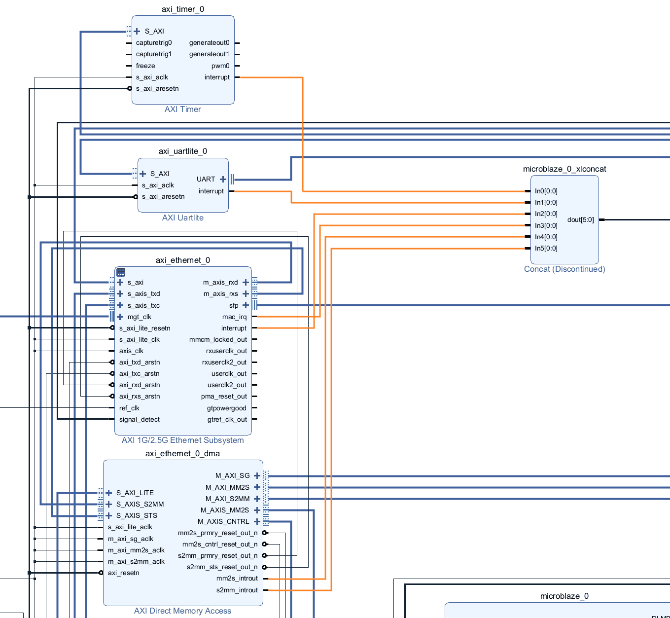
Next step is to connect all the interrupts to the concat block , connect the interrupts from axi timer , axi uartlite , axi ethernet , axi ethernet dma to the concat block
Step 18:
Now the block design is done and the final design should look like the image below
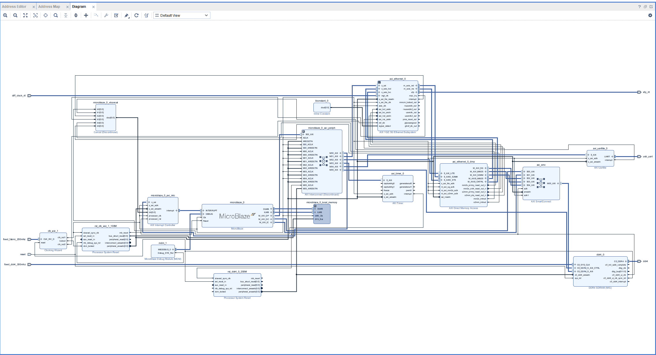
Step 19:
Select the Validate Design option from the Tools menu to ensure that connections are correct.
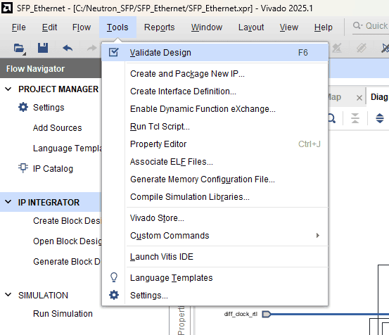
Step 20:
In the Sources window, right-click on the design and select Create HDL Wrapper. Click OK in the dialog box that appears.
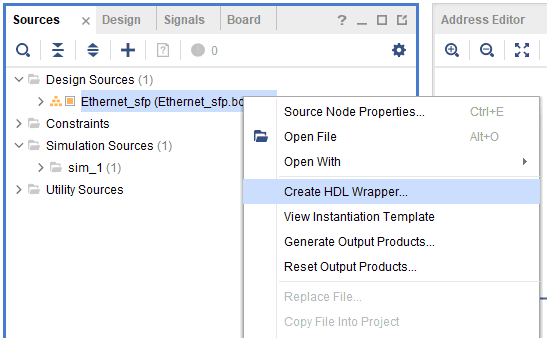
Step 21:
Run synthesis and after synthesis is done open the synthesized design and go to i/o ports tab
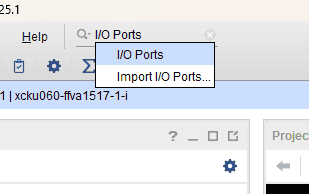
Assign the pin for the GT reference clock for the axi ethernet ip as P32

Save the constraints by cntrl+s ,
now the constraints are saved and go for the implementation and bitstream generation
Step 22:
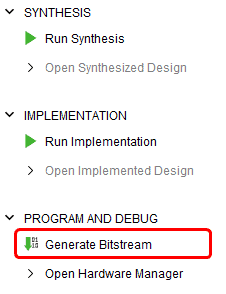
Click Generate Bitstream under the PROGRAM AND DEBUG section of Vivado to synthesize, implement, and generate the bitstream.
Step 22:
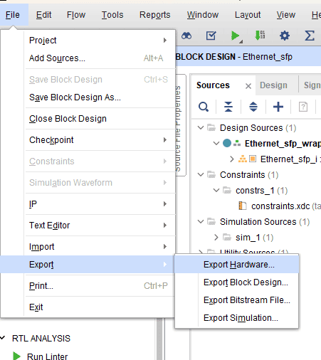
After generating the bitstream successfully, select Export -> Export Hardware from the File menu. Click Next.
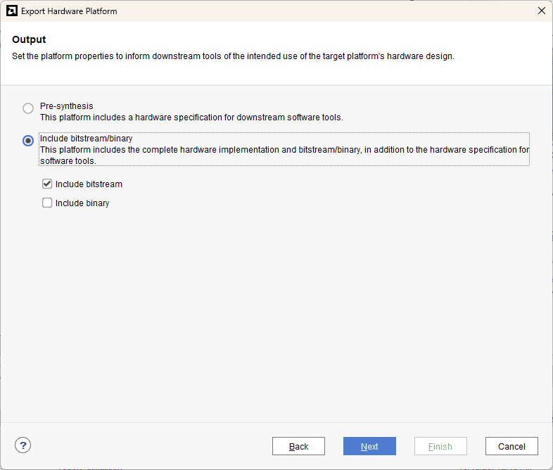
Select the “include bitstream” checkbox and click Next.
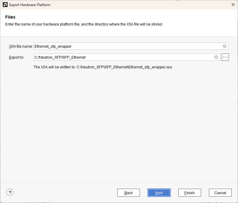
Provide the XSA file name and save it at a suitable location. Click Next and click Finish in the next dialog box.
Step 23:
Launch Vitis Classic.
Note: In Vivado 2024.1, accessing Vitis via the tools menu inadvertently launches Vitis Unified instead of Vitis Classic, which is our preferred tool for project creation. To utilize Vitis Classic, it is necessary to launch it separately.
Step 24:
Creating Separate Vitis Applications for Both FPGA Boards
We will create and configure a separate Vitis application for each Neutron KU60 FPGA board. Each application will be configured with a unique IP address and MAC address to ensure that the boards can be identified individually on the Ethernet network.
One board will operate as the TCP client, initiating a connection to the other board, which will operate as the TCP server and listen for incoming connections on a predefined TCP port. Once the connection is established, the TCP connection supports bidirectional communication, allowing both boards to send and receive messages.
For example, Board 0 can use the IP address 192.168.1.11, while Board 1 can use 192.168.1.10. Both applications will use the lwIP TCP/IP stack to manage network communication, while separate PuTTY terminals will allow us to monitor each board’s output and verify successful data transmission and reception.
This setup enables us to test Ethernet connectivity, bidirectional TCP communication, and data exchange between the two FPGA boards over the SFP optical link.
Step 25:
Note:Only two files differ between the applications for the two FPGA boards. Therefore, the workflow for creating and configuring both Vitis applications remains the same. The source code for each application will be provided separately, with the necessary differences for the respective board
Download the source codes from here.
So first we will create the application for first board we will refer to it as Board 0
In Vitis window, select Create Application Project and click Next in the dialog box that appears.
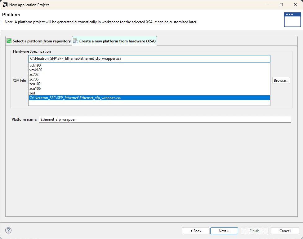
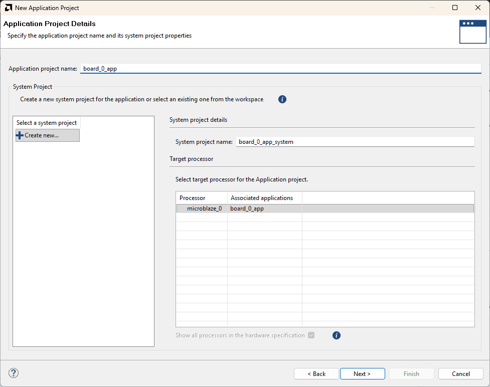
In the Application Project Details window, give an appropriate name for the Vitis Project and click Next. Click Next in the Domain window.
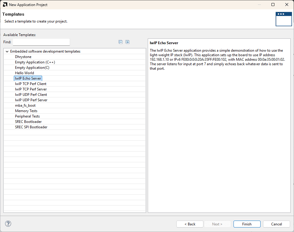
Select the lwIP Echo Server template from the list of available templates and click Finish.
Step 26:
Select Navigate to BSP Settings from Application Project Settings.
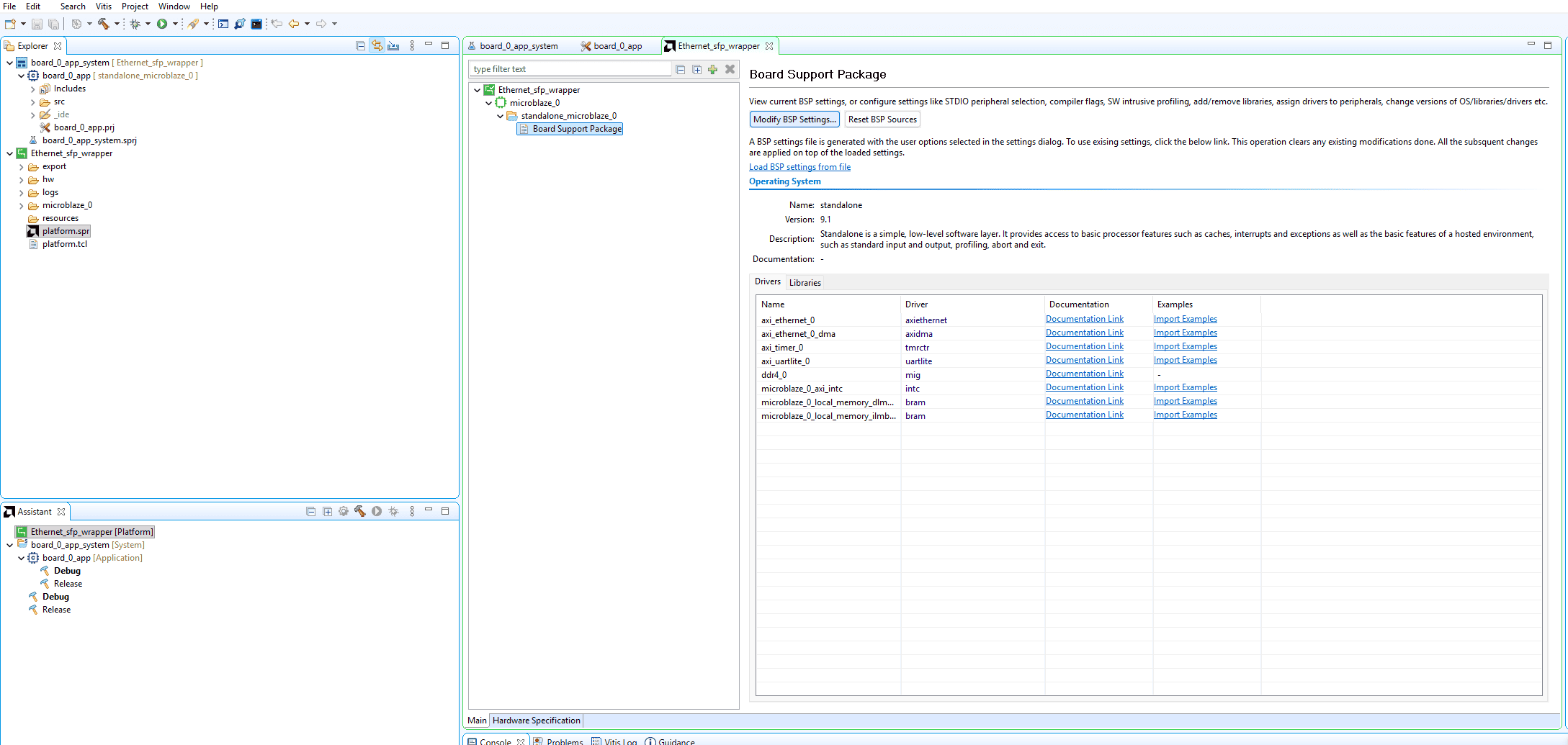
In the Board Support Package Settings window, select lwip (Iwip220) library, change the dhcp_options to “false”, and ensure that “debug options” are “false”.
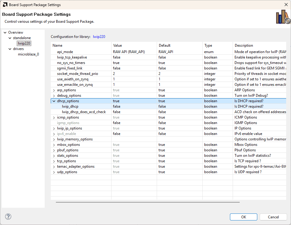
After changing the library settings, click OK.
Step 27:
After creating the Vitis application project, navigate to the src folder within the application project. Two source files must be updated: main.c and echo.c.
Open each file and replace its existing contents with the corresponding Board 0 source code files provided in the project source package. Ensure that the correct Board 0 code is used for both files and that the filenames remain unchanged.
Once both files have been updated, save the changes. The application is now configured with the Board 0-specific code and can proceed to the build and debugging stages.
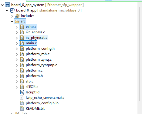
Step 28:
After successfully building the Board 0 application, follow the same workflow to create a separate Vitis application project for Board 1. Replace the contents of main.c and echo.c in the project’s src folder with the corresponding Board 1 source files provided in the project source package. Save the changes and build the application.
Once both Board 0 and Board 1 applications have been built successfully, connect both Neutron KU60 FPGA boards to their respective 12 V DC power supplies and power them on. Ensure that both boards are properly powered and ready for the subsequent Ethernet communication setup and testing.
Step 29:
Programming and Running Both FPGA Boards
After successfully building both Vitis applications, follow the steps below to establish communication between the two Neutron KU60 FPGA boards.
Step 1: Program Board 0
Connect Board 0 to the PC and select the corresponding hardware target in Vitis. Program the FPGA with the appropriate bitstream, then run the Board 0 Vitis application. Ensure that the application uses the Board 0 source code, IP address, and TCP client configuration.
Step 2: Program Board 1
Repeat the same procedure for Board 1. Select its corresponding hardware target, program the FPGA with the appropriate bitstream, and run the Board 1 Vitis application. Ensure that the application uses the Board 1 source code, IP address, and TCP server configuration.
The programming order is not fixed; either board can be programmed first.
Step 3: Open the PuTTY Serial Terminals
Connect both boards to the PC through their USB-UART interfaces. Identify the COM port associated with each board in Windows Device Manager and open two separate PuTTY serial sessions. Configure each session for a baud rate of 9600.
Step 4: Establish Ethernet Communication
Connect the SFP optical modules on both boards using a compatible duplex LC fibre-optic cable. Once both applications are running, monitor the PuTTY terminals for startup messages and TCP connection status.
Step 5: Test Data Exchange
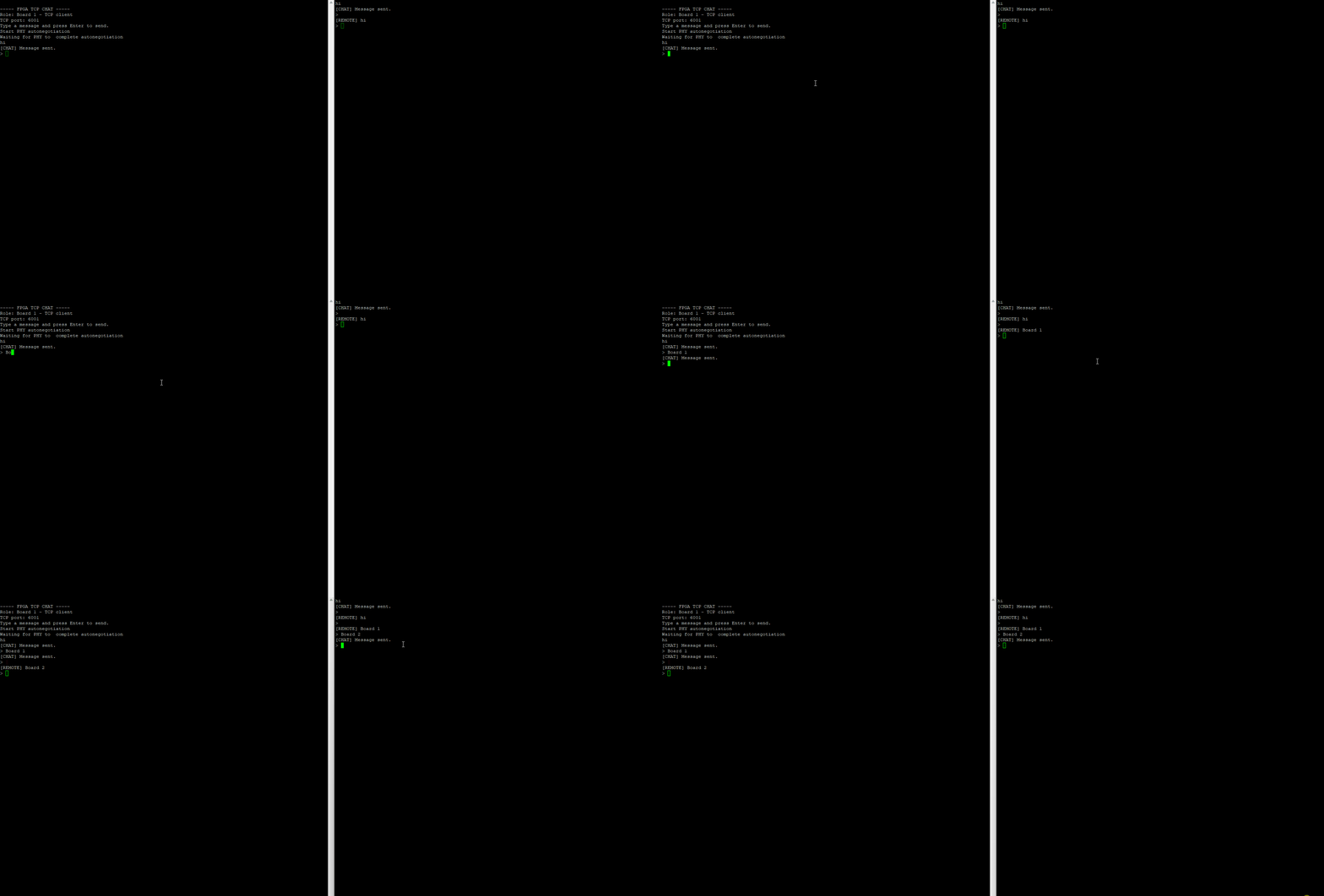
After the TCP connection has been established, type a message into either board’s PuTTY terminal and press Enter. The message should be transmitted over the 1 Gbps Ethernet link using 1000BASE-X and appear in the other board’s terminal. Repeat the test in the opposite direction to verify bidirectional communication.
Successful message exchange confirms that the two FPGA boards can communicate over the SFP optical link using the TCP/IP stack.
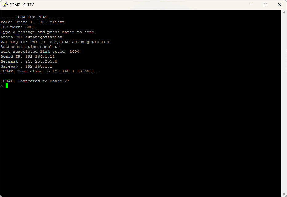
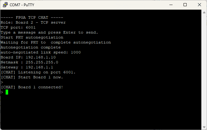
Once both boards have completed initialization and the TCP connection has been established, you can begin testing the communication link. Type a message into the PuTTY terminal connected to either Board 0 or Board 1 and press Enter. The message will be transmitted over the SFP optical fibre link and displayed in the PuTTY terminal of the receiving board.
You can repeat this process in both directions to verify bidirectional TCP communication between the two Neutron KU60 FPGA boards.
Hardware setup: