Introduction
Testing DDR4 memory for Neutron KU60 FPGA Development board involves using specialized tools to ensure the memory functions correctly within the FPGA environment. In Vitis, a software development platform by AMD, a memory test template can be utilized to perform these tests. This template helps in validating the performance and reliability of DDR4 memory by running predefined test patterns and checking for errors. The Purpose of this article is to help readers to understand how to test DDR4 memory available on Neutron KU60 FPGA Board using Memory tests template.
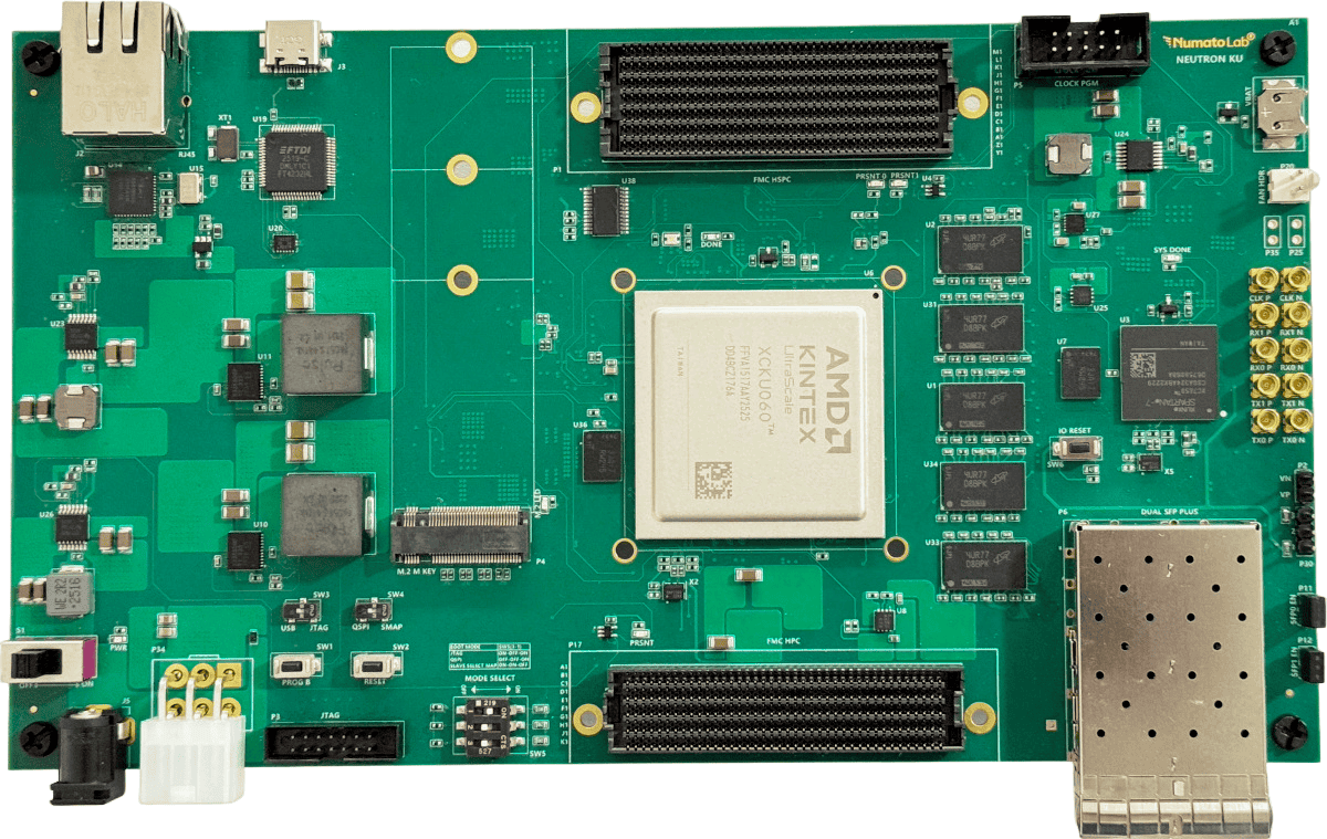
Neutron KU60 FPGA Development Board
The Neutron KU60 FPGA Development Board is a high-performance platform built around the AMD Kintex UltraScale XCKU060 FPGA, designed for demanding high-speed computing, networking, and signal-processing applications. Featuring 5GB ECC-enabled DDR4, dual QSPI configuration memory, multiple clock sources, high-speed SFP+ connectivity, GTH transceiver access, and versatile expansion through FMC+ HSPC, FMC HPC, and an M.2 slot, the board delivers exceptional flexibility for advanced development. With SelectMAP x8, JTAG/USB programming, and programmable clock options, Neutron KU60 provides a robust and adaptable environment for prototyping and deployment.
Prerequisites:
Hardware:
- The Neutron KU60 FPGA Development Board
- USB Type C cable
- 12V DC Power Supply (max 5A current rating)
Software:
- Vivado Design Suite 2025.2.1
- Vitis 2025.2.1
- Serial Terminal (PuTTY, Tera Term, etc.)
Let’s get started
The following steps will walk you through the process of creating a new project with Vivado and building a hardware platform with MicroBlaze soft processor using an IP integrator. Numato Lab’s Neutron KU60 FPGA Development Board is used in this example, but any compatible FPGA platform can be used with minor changes to the steps. Screenshots are added wherever possible to make the process easier for the reader.
Step 1:
Start Vivado Design Suite, and select “Create Project” from the Quick Start section. The project wizard will pop up. Press Next to proceed with creating the project.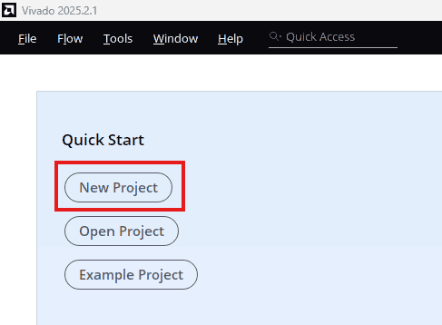
Step 2:
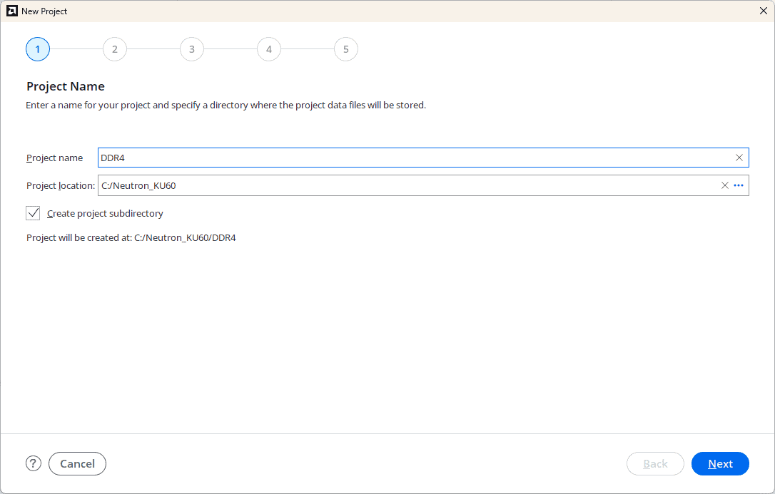
Enter a name for the project and save it at a suitable location. Check the option “Create project subdirectory”. Click Next to continue.
Step 3:
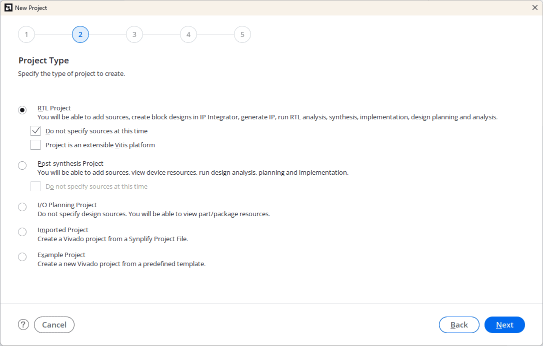
In the Project Type window, select RTL Project and check the option “Do not specify sources at this time”. Click Next.
Step 4:
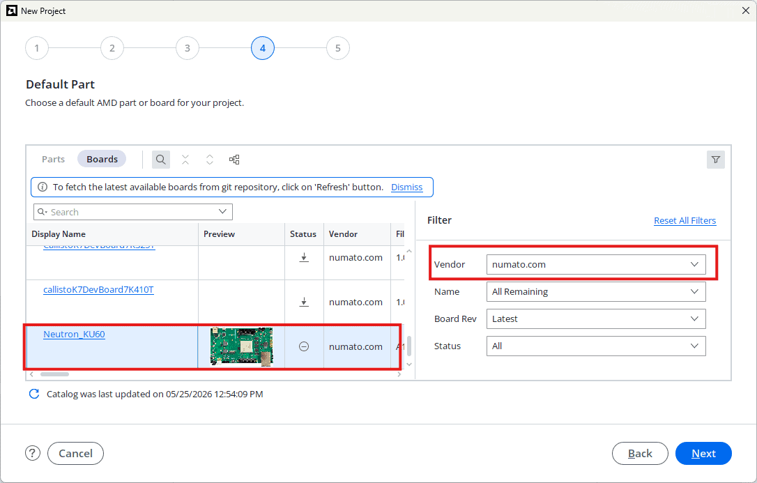
At the “Default Part” stage, switch to the “Boards” tab and set the vendor to numato.com. Select “Neutron_KU60” and click Next. If the Neutron_KU60 does not appear in the list, click “Refresh” to update the board catalog. Vivado will then download the latest board files, after which Neutron_KU60 will become available for selection.
Continue the wizard and finish creating the project. When the new project wizard exits, a new project will be opened up in Vivado with the settings you have selected.
Step 5:
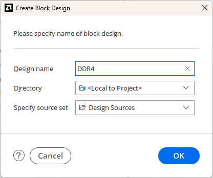
In the Flow Navigator panel, select Create Block Design under IP INTEGRATOR. Enter a name for the block design and click OK. An empty block design will be created.
Step 6:
Click the Board tab. The default peripherals available for the Neutron_KU60 will be displayed. (If the “Board” tab is not visible, search for it using the search option in Vivado.)
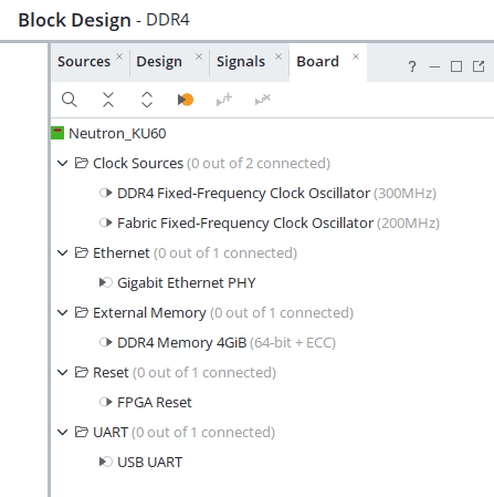
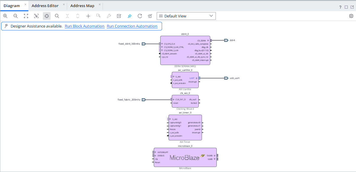
Drag and drop DDR4 Memory 4GiB, Fabric Fixed-Frequency Clock Oscillator and USB UART into IP Canvas.
Step 7:
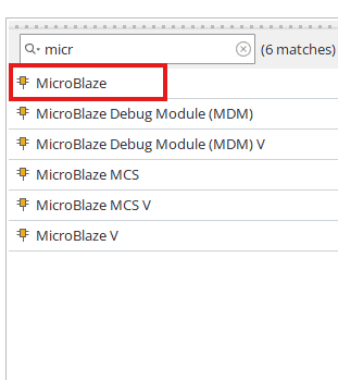
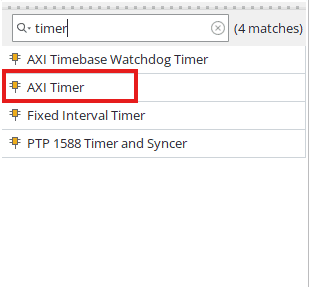
In the Diagram window, right-click and select “Add IP” from the pop-up menu. Search for “MicroBlaze” & “AXI Timer” and add them to the design by double-clicking them.
Step 8:
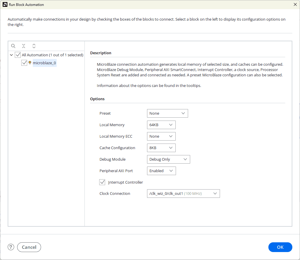
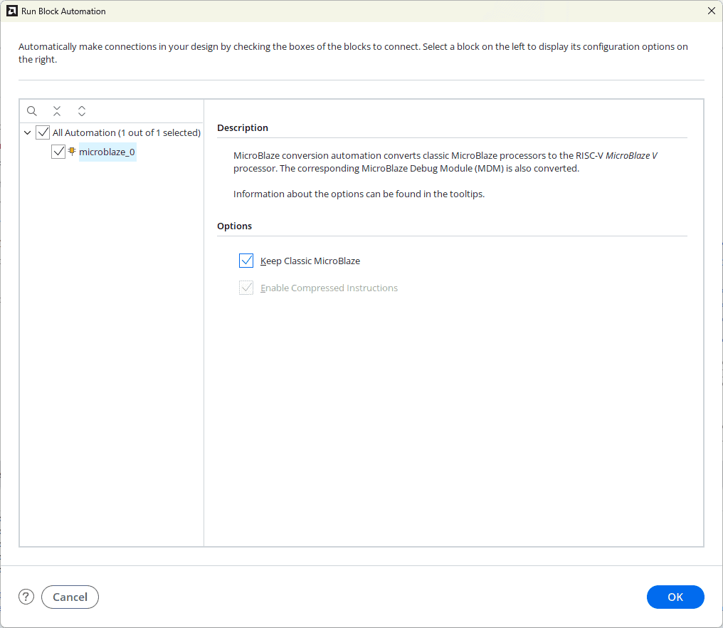
Click “Run Block Automation” present in the “Designer Assistance available” bar on the top left corner of the window to complete the design. Select the settings as shown in the following image. Click “OK” for Vivado to automatically configure the blocks for you. Once Block Automation is complete, run “Connection Automation” so Vivado can connect the blocks to make a complete system.
Enable the “Interrupt controller” in the Run Block Automation Window as below
Step 9:
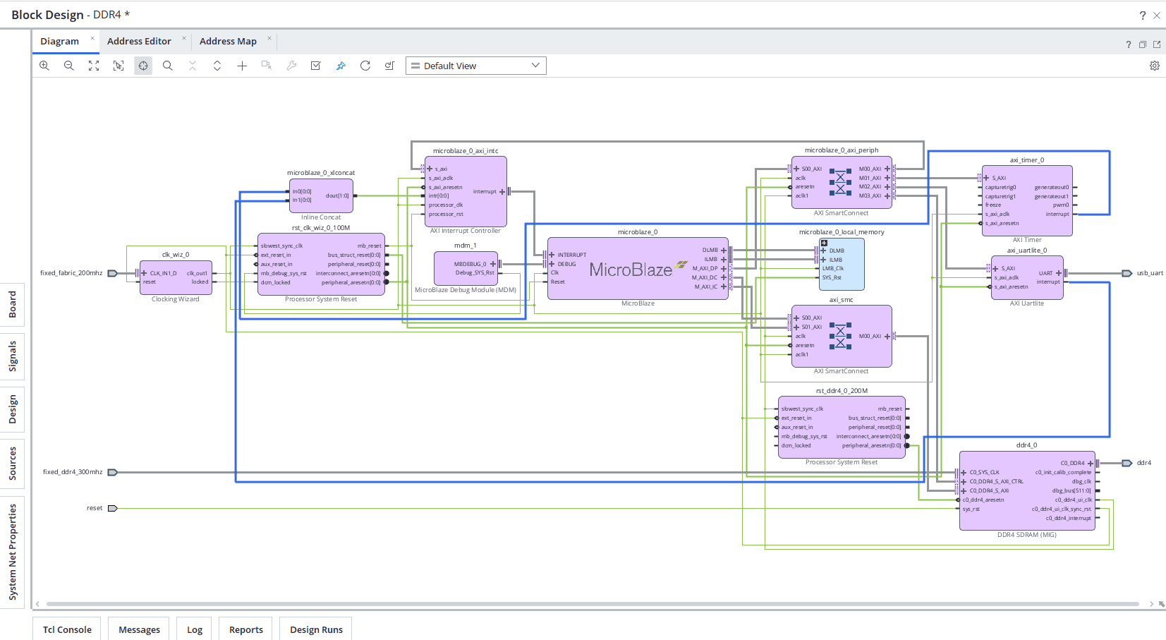
Connect interrupt output lines from “AXI Timer” and “UARTLite” to the “Concat” block as shown in the figure. Select the “Validate Design” option from the Tools menu to make sure that connections are correct.
Step 10:
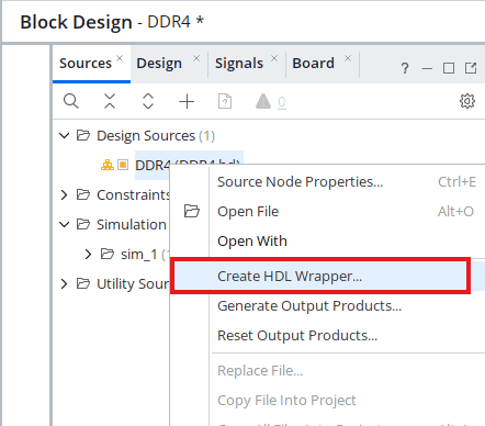
Right-click “ddr4_test” in the “Sources” window, and select “Create HDL Wrapper” from the pop-up menu. Click “OK” on the window that appears to finish generating a wrapper.
Step 11:
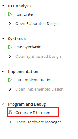
Click “Generate Bitstream” under the “Program and Debug” section to synthesize, implement, and generate a bitstream.
Step 12:
After generating the bitstream successfully, select Export -> Export Hardware from the File menu. Click Next.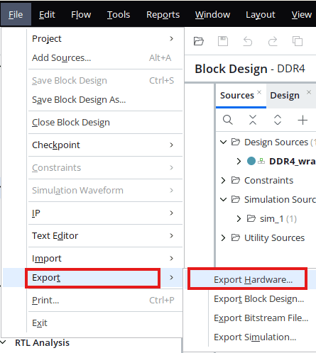
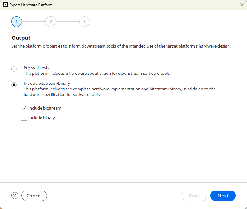
Select the “include bitstream” checkbox and click Next.
Provide the XSA file name and save it at a suitable location. Click Next and click Finish in the next dialog box.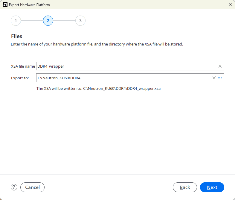
Step 13:
Launch the Vitis IDE from the Tools section in Vivado.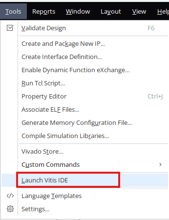
Step 14:
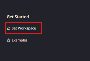
After launching the Vitis IDE, create a new workspace directory where the Vitis project will be stored.
Step 15:
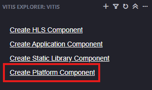
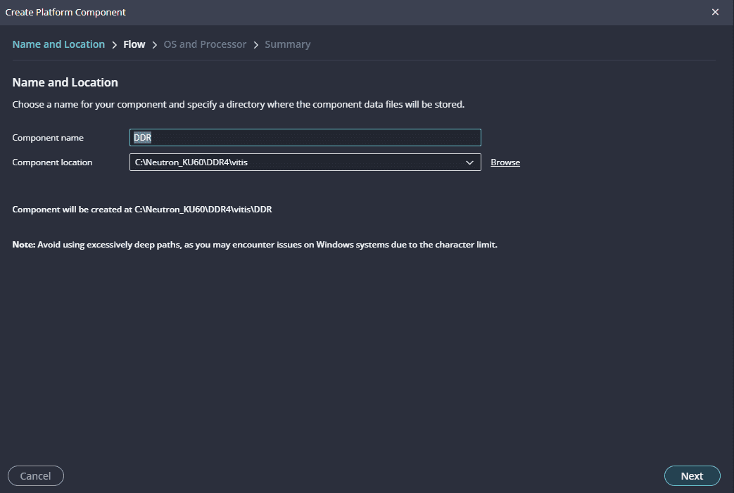
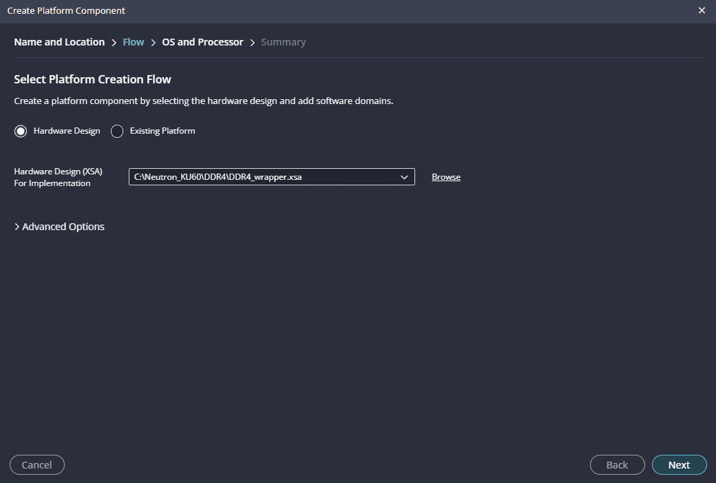
After setting the workspace, create a new platform for the project, by selecting “Create Platform Component”, click “Next”, in the Flow tab select the XSA file saved using the step 12 and finally click “Next” and “Finish” respectively.
After successful creation of the platform, build the platform.
Step 16:
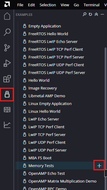
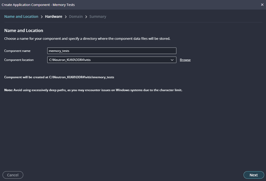
Next create the Memory Test Application component by selecting the “Memory Tests” template from the “examples”.
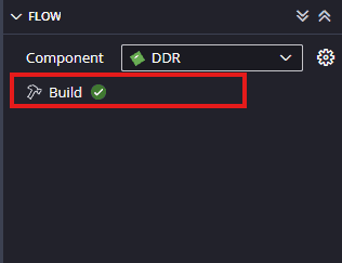
When the memory tests project is added successfully, build the project manually.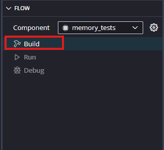
Step 17:
Once the build is completed successfully, Power up the Neutron KU60 and connect the JTAG or USB-JTAG to the board. Follow the steps mentioned under Programming Neutron KU60 FPGA Development Board Using USB-JTAG in the product user manual. Open any serial terminal program (such as PuTTY, Teraterm, etc.) and open the port corresponding to Neutron KU60 with a 9600 baud rate (the default baud rate given in UART IP).
Step 18:
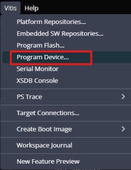
Program the Kintex Ultrascale (KU60) FPGA on Neutron KU60 with a simple boot loop program by selecting the Program Device option from the Vitis menu.
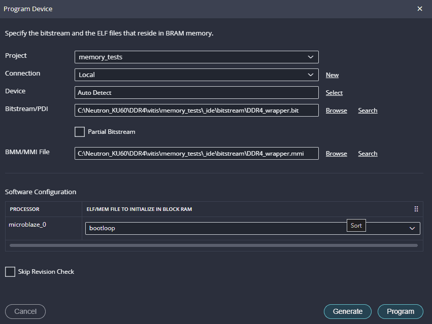
Once the “Program Device” window opens give the path for .bit and .mmi files .
If the “BMM/MMI” File is not selected , manually browse and select the file .Once the files are selected click on “Program” .
Step 19:
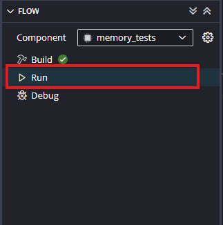
Run the application by selecting the “Run”.
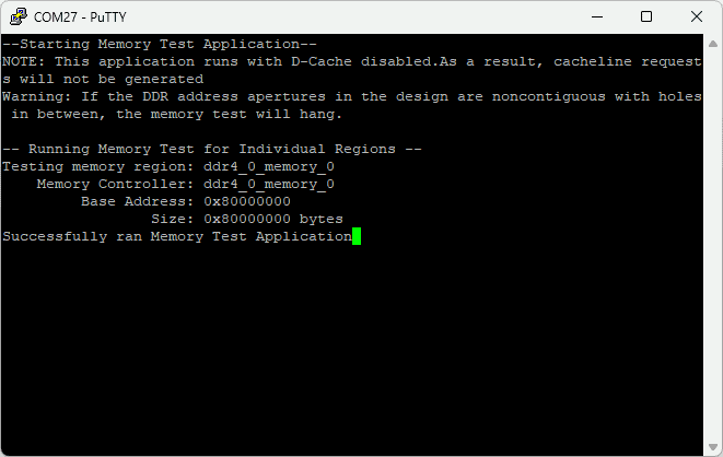
Step 20:
If everything went well, the Memory tests application running on the board should start printing the Memory tests over the UART and the output should be displayed on the Serial Terminal application as shown in the image below.