
Introduction
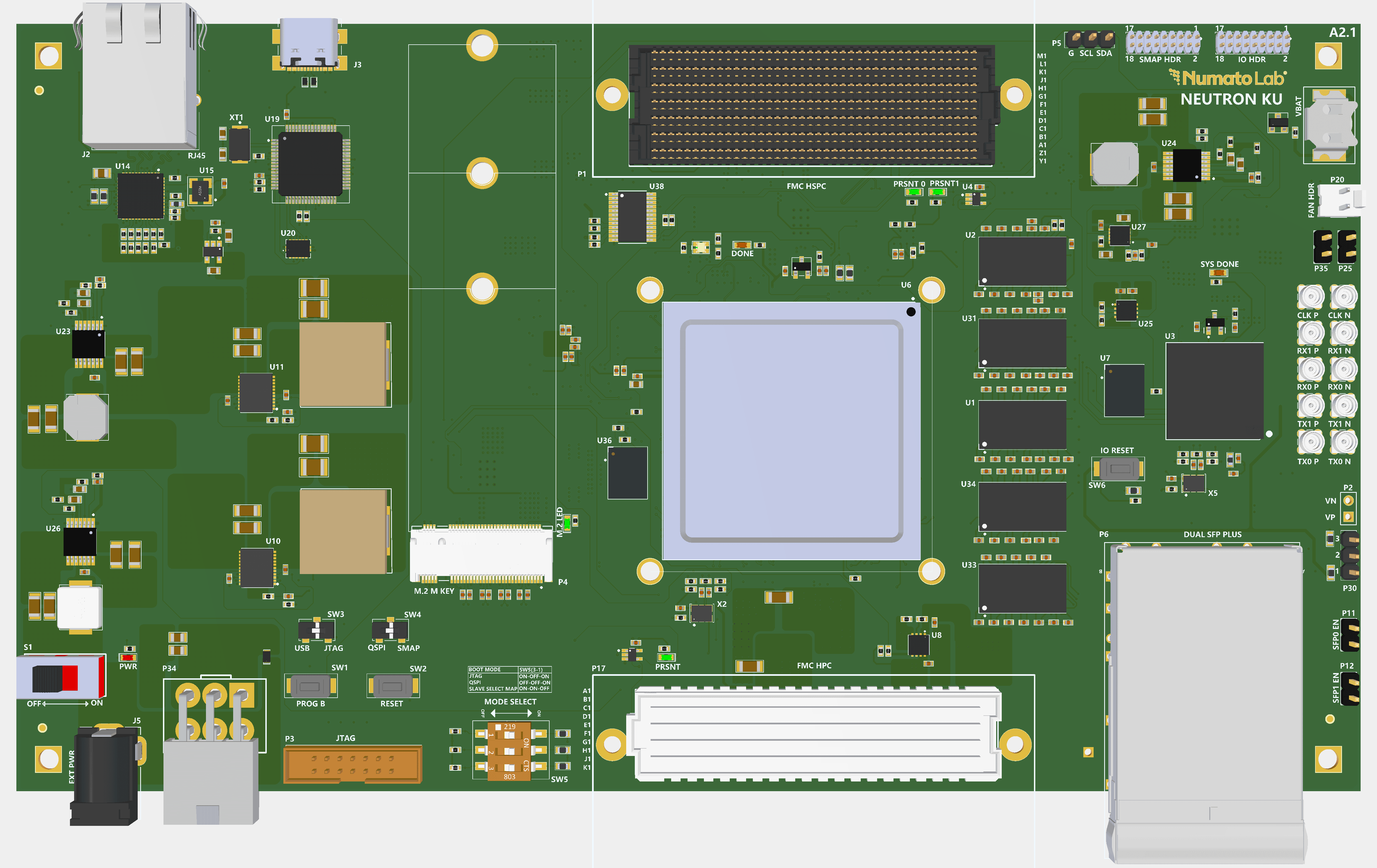
The Neutron KU60 Development Board is a multi-FPGA platform designed to support flexible system configuration, control, and high-speed inter-device communication. In the Neutron architecture, the Kintex UltraScale FPGA (XCKU060-1FFVA1517I) serves as the high-performance processing device, while the Spartan-7 FPGA (XC7S50-1CSGA324C) is used for system management and configuration control (system controller).
The on-board Spartan-7 FPGA functions as the system controller for SelectMAP-based configuration of the Kintex UltraScale KU60 FPGA. It operates in SelectMAP master mode, managing the parallel configuration interface and generating the configuration clock (CCLK).
The SelectMAP configuration interface is a parallel configuration mode used for programming AMD FPGAs, enabling high-throughput bitstream transfer under external master control. In this configuration scheme, the Spartan-7 FPGA operates as the configuration master, controlling the configuration sequence, while the Kintex UltraScale FPGA functions as the slave device, receiving configuration data and control signals through the SelectMAP interface.
Block Design
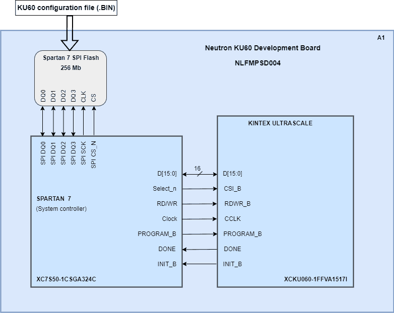
This diagram illustrates the master-slave configuration relationship where Spartan-7 controls KU60 programming through a dedicated 8-bit/16-bit parallel bus with key control and status signals.
SelectMAP
In the Neutron KU60 FPGA development board, the Spartan-7 FPGA operates as the system controller and SelectMAP master, responsible for configuring the Kintex UltraScale KU60 FPGA.
The configuration is performed using the SelectMAP interface in parallel mode (e.g., x8 & x16mode), where the Spartan-7 generates the configuration clock (CCLK) and drives the data bus. It controls configuration signals such as PROGRAM_B and monitors INIT_B and DONE to manage and verify the configuration process.
The Spartan-7 reads the configuration bitstream from onboard memory and transfers it to the KU60, ensuring proper sequencing and error handling during configuration.
| Sl. No. | SelectMAP Pin Name | KU060 Pin | Spartan 7 Pin |
|---|---|---|---|
| 1 | DONE | AF11 | V14 |
| 2 | INIT_B | R11 | P13 |
| 3 | RDWR | AB9 | U17 |
| 4 | CSI_B | AL15 | U16 |
| 5 | PROGRAM_B | AA9 | V15 |
| 6 | CCLK | AC11 | R16 |
| 7 | DATA0 | AE11 | R14 |
| 8 | DATA1 | AD10 | T14 |
| 9 | DATA2 | AC9 | N15 |
| 10 | DATA3 | AD9 | P16 |
| 11 | DATA4 | AF14 | L17 |
| 12 | DATA5 | AG14 | L18 |
| 13 | DATA6 | AE13 | M14 |
| 14 | DATA7 | AF13 | N14 |
| 15 | DATA8 | AF15 | N13 |
| 16 | DATA9 | AG15 | M16 |
| 17 | DATA10 | AG12 | M17 |
| 18 | DATA11 | AH12 | M18 |
| 19 | DATA12 | AK13 | N18 |
| 20 | DATA13 | AK12 | P18 |
| 21 | DATA14 | AH13 | R18 |
| 22 | DATA15 | AJ13 | T18 |
SelectMAP Configuration Procedure
In the Neutron KU60 development board, the KU60 FPGA is configured using the SelectMAP interface, where the Spartan-7 FPGA acts as the configuration master and the KU60 operates as the slave device. The configuration bitstream (.bin file) for the KU60 is pre-stored in the QSPI flash memory connected to the Spartan-7.
The configuration process is initiated by the Spartan-7 through a bootloader application developed in Vitis. This application reads the bitstream data and its size from the external memory and prepares the SelectMAP interface for data transfer. The KU60 configuration logic is first reset by asserting the PROGRAM_B signal, and the interface control signals such as RDWR_B (set to write mode) and CSI_B (chip select) are configured accordingly. The system then waits for the INIT_B signal from the KU60 to go High, indicating that the device is ready to receive configuration data.
Once initialization is complete, the Spartan-7 begins transferring the bitstream to the KU60 over the parallel SelectMAP data bus. The data is sent sequentially in synchronization with the configuration clock (CCLK), ensuring proper timing and reliable communication. During this phase, the INIT_B signal is continuously monitored to detect any configuration errors that may occur while transmitting the bitstream.
After the complete bitstream has been successfully transmitted, additional clock cycles are provided to finalize the startup sequence. The DONE signal from the KU60 is then monitored to confirm successful configuration. A High state on the DONE signal indicates that the FPGA has been properly programmed and is ready for normal operation. This SelectMAP-based approach enables efficient, high-speed configuration of the KU60 FPGA under the control of the Spartan-7 master device.
Generating BIN File for SelectMAP Configuration
Step 1:
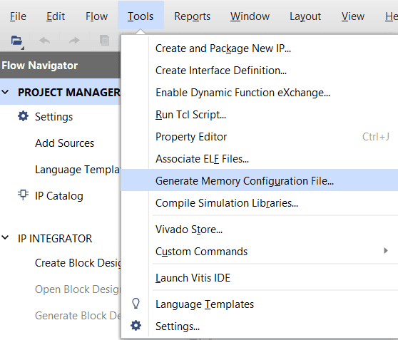
In Vivado, open the Generate Memory Configuration File utility from:
Tools → Generate Memory Configuration File
Step 2:
Select the file Format as BIN and choose the exact SPI Flash Memory Part used in the design. Provide a suitable name for the output file.
Enable Load bitstream files and add the generated download.bit file. Place the SelectMAP bootloader bitstream at the required flash start address and allocate the application BIN/bitstream file to a different flash location with sufficient reserved memory space.
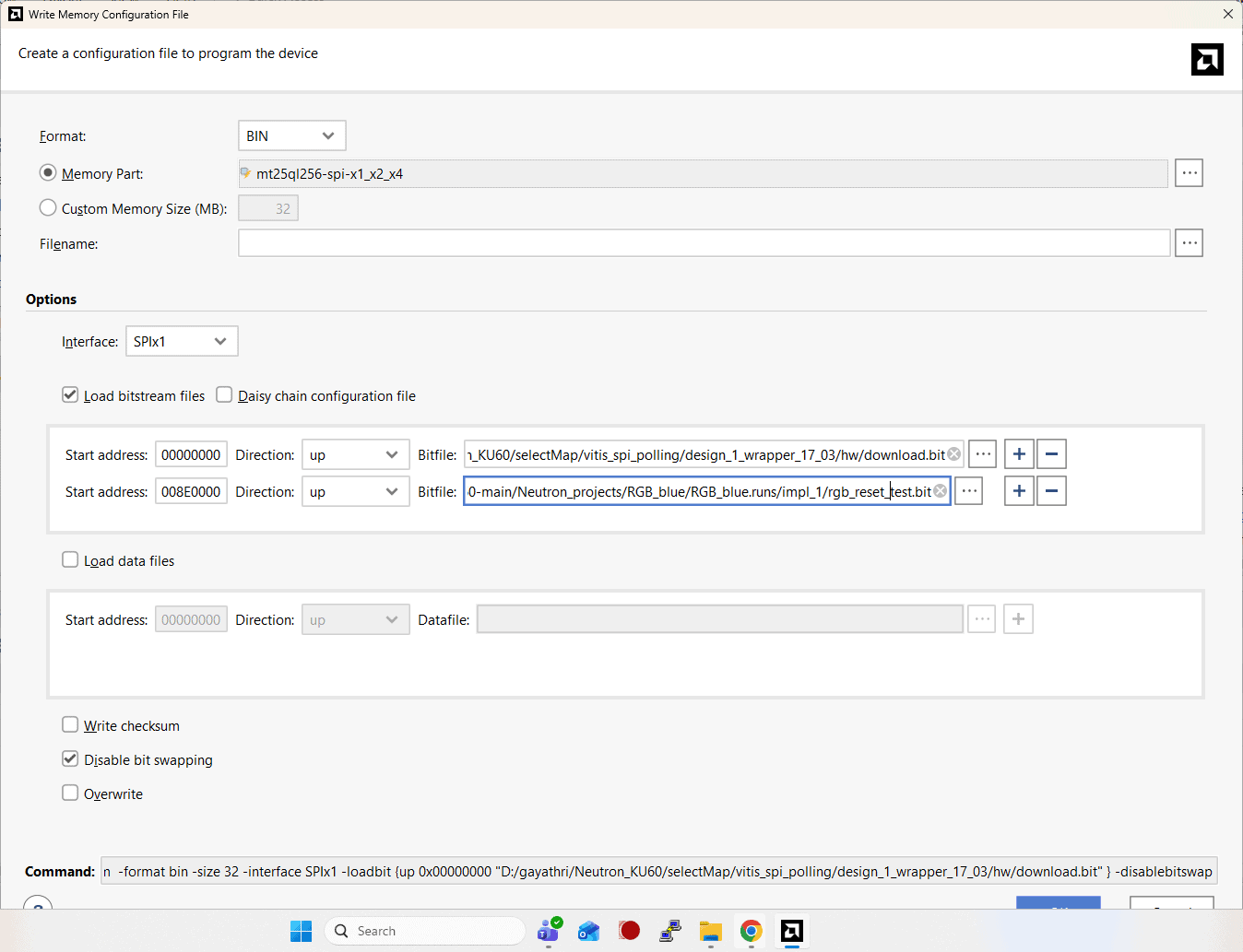
Check Disable bit swapping, as this setting is mandatory for proper SelectMAP data transfer.
Step 3:
Verify all the settings and click OK or Generate to create the BIN file for the SelectMAP-based FPGA configuration.
System Controller Hardware Interfaces
Quad SPI FLASH
Quad SPI NOR flash memory device (MT25QL256ABA8E12-0AAT) is connected to the Spartan 7 FPGA, with a capacity of 256 Mbit.
The flash memory operates at 3.3 V and is used for FPGA configuration storage and non-volatile data storage.
| Bank | FPGA Pin | Signal Name | Function |
|---|---|---|---|
| 14 | K17 | IO_L1P_T0_D00_MOSI_14 | SPI_DQ0 |
| 14 | K18 | IO_L1N_T0_D01_DIN_14 | SPI_DQ1 |
| 14 | L14 | IO_L2P_T0_D02_14 | SPI_DQ2 |
| 14 | M15 | IO_L2N_T0_D03_14 | SPI_DQ3 |
| 14 | M13 | IO_L6P_T0_FCS_B_1 | SPI_CS_N |
| 14 | P14 | IO_L11P_T1_SRCC_14 | SPI_RST |
| 0 | C8 | CCLK_0 | SPI_SCK |
IO reset switch
The Spartan 7 FPGA has a Push-button SW6, typically used as a “Reset” signal for designs running on the FPGA. Push-button SW6 is connected to FPGA pin T12. Push-button SW6 is active-high. This pushbutton can also be used for any other input and is not just limited to being used as a Reset signal.
System clock
The Spartan-7 System Controller is provided with a dedicated 200 MHz differential system clock (P: D14, N: D14). This clock ensures stable and reliable operation of the system controller functions, including FPGA configuration and system management tasks.
UART
The board uses an FTDI FT4232HL USB interface device.
Channel B of the FTDI is configured as a UART interface, and the associated signal connections are listed below.
| Bank | FPGA pin | Signal name | Function |
|---|---|---|---|
| 14 | U12 | IO_L21P_T3_DQS_14 | TXD |
| 14 | V13 | IO_L21N_T3_DQS_D22_14 | RXD |
Contact us for more details about the system controller.
User IO Header
The Spartan-7 FPGA provides a 6-pair differential user I/O header connected to Bank 35, which operates at an I/O voltage of 3.3 V. These pins can be configured as differential or single-ended general-purpose I/O (GPIO) and may be used to interface with external modules, custom hardware, or other user-defined peripherals. The pin assignments for the user I/O header are provided in the table below.
| Pin No. On The Header | Header Pin Name | FPGA PIN | Pin description | Pin No. On The Header | Header Pin Name | FPGA PIN | Pin description |
|---|---|---|---|---|---|---|---|
| 1 | VCCIO_3V3 | VCCIO_3V3 | 2 | VCC | |||
| 3 | IO1_35_P | C3 | IO_L8P_T1_AD14P_35 | 4 | IO0_35_P | C4 | IO_L7P_T1_AD6P_35 |
| 5 | IO1_35_N | B3 | IO_L8P_T1_AD14N_35 | 6 | IO0_35_N | B4 | IO_L7P_T1_AD6N_35 |
| 7 | IO3_35_P | F4 | IO_L13P_T2_MRCC_35 | 8 | IO2_35_P | C1 | IO_L12P_T1_MRCC_35 |
| 9 | IO3_35_N | E4 | IO_L13N_T2_MRCC_35 | 10 | IO2_35_N | B1 | IO_L12N_T1_MRCC_35 |
| 11 | IO5_35_P | H5 | IO_L22P_T3_35 | 12 | IO4_35_P | G2 | IO_L21P_T3_DQS_35 |
| 13 | IO5_35_N | H4 | IO_L22N_T3_35 | 14 | IO4_35_N | G1 | IO_L21N_T3_DQS_35 |
| 15 | GND | GND | 16 | GND | GND | ||
| 17 | GND | GND | 18 | GND | GND |
SelectMap Header (SMAP HDR)
The board provides a dedicated SelectMAP x8 header that exposes the FPGA’s SelectMAP x8 interface signals for external connectivity. The pin assignments for the SelectMAP x8 header are provided in the table below.
| Pin No. On The Header | Header Pin Name | Spartan FPGA PIN | FPGA Pin Description | KU FPGA PIN | FPGA Pin Description | Pin No. On The Header | Header Pin Name | Spartan FPGA PIN | FPGA Pin Description | KU FPGA PIN | FPGA Pin Description |
|---|---|---|---|---|---|---|---|---|---|---|---|
| 1 | VCCIO_3V3 | VCCIO_3V3 | 2 | VCC | |||||||
| 3 | DATA1 | T14 | IO_L13N_T2_MRCC_14 | AD10 | D01_DIN_0 | 4 | DATA0 | R14 | IO_L13P_T2_MRCC_14 | AE11 | D00_MOSI_0 |
| 5 | DATA3 | P16 | IO_L12N_T1_MRCC_14 | AD9 | D03_0 | 6 | DATA2 | N15 | IO_L12P_T1_MRCC_14 | AC9 | D02_0 |
| 7 | DATA5 | L18 | IO_L4N_T0_D05_14 | AG14 | IO_L22N_T3U_N7_DBC_AD0N_D05_65 | 8 | DATA4 | L17 | IO_L4P_T0_D04_14 | AF14 | IO_L22P_T3U_N6_DBC_AD0P_D04_65 |
| 9 | DATA7 | N14 | IO_L5N_T0_D07_14 | AF13 | IO_L21N_T3L_N5_AD8N_D07_65 | 10 | DATA6 | M14 | IO_L5P_T0_D06_14 | AE13 | IO_L21P_T3L_N4_AD8P_D06_65 |
| 11 | RDWR | U17 | IO_L15P_T2_DQS_RDWR_B_14 | AB9 | RDWR_FCS_B_0 | 12 | INIT_B | P13 | IO_L19P_T3_D26_14 | R11 | INIT_B_0 |
| 13 | CSI_B | U16 | IO_L16P_T2_CSI_B_14 | AL15 | IO_T2U_N12_CSI_ADV_B_65 | 14 | DONE | V14 | IO_L20P_T3_D24_14 | AF11 | DONE_0 |
| 15 | PROGRAM_B | V15 | IO_L20N_T3_D23_14 | AA9 | PROGRAM_B_0 | 16 | SYS_CCLK | R16 | IO_L14P_T2_SRCC_14 | AC11 | CCLK_0 |
| 17 | GND | GND | 18 | GND | GND |