

1.FPIC Overview and Introduction
1.1.Overview
FPIC (FPGA Peripheral Interface Connector) is a standardized interface developed by Numato Systems Pvt Ltd for connecting peripheral modules to FPGA-based carrier boards. It establishes a defined mechanical, electrical, and signalling framework that enables developers to expand the functionality of FPGA platforms through modular hardware.
The FPIC standard integrates user-configurable I/O signals, differential signal pairs, power supply rails, and optional high-speed transceiver interfaces. Different FPIC variants use different connector families and pitches to accommodate their respective interface requirements. FPIC-ST uses the QTE/QSE connector family, whereas FPIC-GT4 and FPIC-GT8 use the QTH/QSH connector family.
FPIC supports three module variants: FPIC-ST, FPIC-GT4, and FPIC-GT8. Each variant offers different electrical and high-speed interface capabilities to meet varying application requirements.
 Was this helpful?

1.2.Purpose and Objectives
The primary objective of the FPIC standard is to provide a unified, reliable, and high-performance interface for modular expansion of FPGA-based systems. By defining connector arrangements, pin assignments, mechanical dimensions, and electrical requirements, FPIC helps hardware developers design compatible peripheral modules and carrier boards.
The key objectives of the FPIC standard are:
- Standardized connectivity: Establish defined interfaces between FPGA carrier boards and peripheral modules.
- Flexible I/O integration: Support single-ended and differential I/O interfaces, subject to the capabilities of the FPGA and system implementation.
- High-speed communication: Support FPGA transceiver-based applications requiring multi-gigabit serial connectivity.
- Defined mechanical interfaces: Specify connector requirements, module dimensions, mounting arrangements, and component clearance requirements for each applicable variant.
- Hardware interoperability: Define common electrical and signaling requirements to facilitate the development of compatible modules and carriers.
- Scalable interface options: Provide different module variants to support general-purpose I/O applications and high-speed transceiver-based designs.
The FPIC standard is designed to support high-speed serial data rates of up to 10 Gb/s per differential lane and single-ended or differential I/O signalling rates of up to 2 Gb/s, subject to the capabilities of the selected FPGA, connector, and overall system implementation.
2.FPIC Module Variants
The FPIC standard defines three module variants: FPIC-ST, FPIC-GT4, and FPIC-GT8. Each variant is designed to address different FPGA peripheral interface requirements, offering different user I/O configurations and high-speed transceiver capabilities.
The variants differ in their connector interfaces, signal assignments, and supported functionality. Selecting the appropriate variant depends on the required I/O resources, high-speed connectivity, and the FPIC carrier board being used.
2.1.FPIC-ST
USER I/O
- 24 differential I/O pairs (48 single-ended signals)
- 8 clock-capable I/O pairs
CARRIER-SIDE CONNECTOR
Samtec QSE-040-01-F-D-A
MODULE-SIDE CONNECTOR
Samtec QTE-040-02-F-D-A
PCB DESIGN FILES
FPIC PCB Templates
2.2.FPIC-GT4
USER I/O
- 16 differential I/O pairs (32 single-ended signals)
- 4 clock-capable I/O pairs
GT TRANSCEIVER LANES
- 4 GT lanes (GT0–GT3)
- 1 differential GT reference clock pair (REF_CLK0)
CARRIER-SIDE CONNECTOR
Samtec QSH-040-01-L-D-DP-A
MODULE-SIDE CONNECTOR
Samtec QTH-040-02-L-D-DP-A
PCB DESIGN FILES
FPIC PCB Templates
2.3.FPIC-GT8
USER I/O
- 16 differential I/O pairs (32 single-ended signals)
- 4 clock-capable I/O pairs
GT TRANSCEIVER LANES
- 8 GT lanes (GT0–GT7)
- 2 differential reference clock pairs (REF_CLK0 and REF_CLK1)
CARRIER-SIDE CONNECTOR
Samtec QSH-040-01-L-D-DP-A
MODULE-SIDE CONNECTOR
Samtec QTH-040-02-L-D-DP-A
PCB DESIGN FILES
FPIC PCB Templates
3.Connector Specifications
FPIC variants use different connector families and pitches. FPIC-ST uses the QTE/QSE connector family, while FPIC-GT4 and FPIC-GT8 use the QTH/QSH connector family.
| Parameter | FPIC-ST | FPIC-GT4 / GT8 |
|---|---|---|
| Carrier connector | Samtec QSE-040-01-F-D-A | Samtec QSH-040-01-L-D-DP-A |
| Module connector | Samtec QTE-040-02-F-D-A | Samtec QTH-040-02-L-D-DP-A |
| Positions | 80 | 80 |
| Connector pitch | 0.80 mm | 0.50 mm |
| Mounting | Surface mount | Surface mount |
| Standard stacking height | 8 mm | 8 mm |
4.FPIC Modules and Carrier Boards
This section provides a list of available FPIC peripheral modules and carrier boards developed by Numato. Refer to the respective product pages for detailed specifications, supported interfaces, features, and technical resources.
5.FPIC Module
5.1.FPIC Module Dimensions
5.1.1.FPIC-ST Module Dimensions
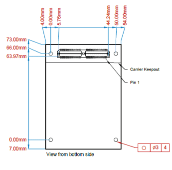
The FPIC-ST module has an overall PCB dimension of 58.0mm × 80.0mm and incorporates four Ø3.0mm mounting holes located 4.0mm from the side edges and 7.0mm from the top and bottom edges.
5.1.2.FPIC-GT4 / GT8 Module Dimensions
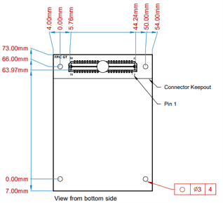
The FPIC GT4 & GT8 module has an overall PCB dimension of 58.0mm × 80.0mm and incorporates four Ø3.0mm mounting holes located 4.0mm from the side edges and 7.0mm from the top and bottom edges.
5.2.FPIC Air-Cooled Module Dimensions
5.2.1.FPIC-ST Air-Cooled Module Dimensions
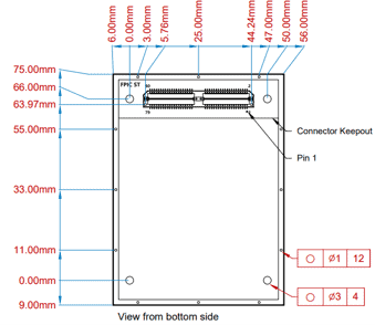
The FPIC-ST Air Cooled module has an overall PCB dimension of 62.0mm × 84.0mm and incorporates four Ø3.0mm mounting holes located 6.0mm from the side edges and 9.0mm from the top and bottom edges.
5.2.2.FPIC-GT4/GT8 Air-Cooled Module Dimensions
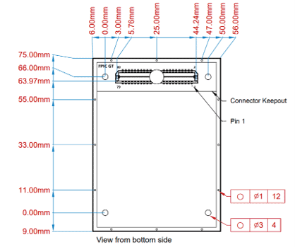
The FPIC GT4 & GT8 Air Cooled module has an overall PCB dimension of 62.0mm × 84.0mm and incorporates four Ø3.0mm mounting holes located 6.0mm from the side edges and 9.0mm from the top and bottom edges.
6.FPIC Carrier
The FPIC carrier is the FPGA main board that hosts one or more FPIC connector sites and supplies power, clock, and I/O resources to installed modules. The carrier SHALL implement the power sequencing, VIO Selection, and presence detection protocols defined in this standard.
6.1.FPIC Carrier Dimensions
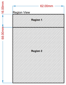
The dimensions of the FPIC carrier board SHALL be sufficient to accommodate one or more FPIC connectors, as required by the intended application. The mechanical mounting hole locations and hole diameters SHALL match the corresponding FPIC module specification to ensure mechanical compatibility. When an FPIC module is intended to be mounted at the edge of the carrier PCB, the Region 1 dimensions SHALL be implemented without deviation. When the FPIC module is mounted away from the PCB edge, both Region 1 and Region 2 dimensions SHALL be implemented in accordance with this specification. For half-width FPIC modules, the mounting holes SHALL be positioned 4.0mm from the side edge and 9.0mm from the top and bottom edges of the module, as defined in the corresponding mechanical drawing. (Refer Component Height Envelopes section for region details)
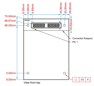
FPIC-ST carrier Dimension
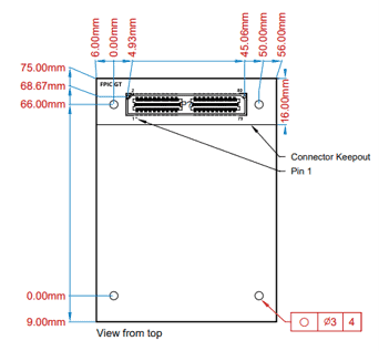
FPIC-GT carrier Dimension
6.2.Multiple connector placement requirements
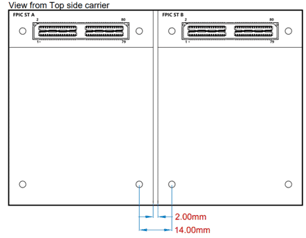
For designs incorporating multiple FPIC connectors, the connector-to-connector spacing SHALL meet the minimum mechanical clearance requirements specified in the below figure to ensure proper module installation, removal, and mechanical compatibility.
6.3.Component Height Envelopes
| Region | Maximum Height — Commercial | Maximum Height — Commercial |
|---|---|---|
| Region 1 (connector side) — connector zone | Connector protrusion only | Connector protrusion only |
| Region 2 — component zone top | 16mm above PCB surface | 12mm above PCB surface |
| Region 2 — component zone bottom (Below PCB surface) | • 3.4mm for 5mm stacking height. • 6.5mm for 8mm stacking height. • 9.5mm for 11mm stacking height. | • 3.4mm for 5mm stacking height. • 6.5mm for 8mm stacking height. • 9.5mm for 11mm stacking height. |
NOTE:
Region 2 defines the available component placement area on the module. The 66.0mm dimension shown in the figure is for reference only and does not represent a fixed requirement. The actual length of region 2 may be reduced depending on the component placement and the overall module design. Designers may also implement half-width modules, provided that the required corner mounting holes and their specified locations are maintained to ensure mechanical compatibility with the carrier.
7.Carrier and Module Connection
FPIC modules connect to the corresponding FPIC connectors on the carrier board. Correct connector placement, mechanical alignment, and power-good signaling are essential for reliable operation.
7.1.Carrier and Module Placement
The FPIC carrier connector may be placed along the edge of the carrier PCB or away from the PCB edge, as illustrated below. The connector placement and mounting-hole arrangement shall follow the mechanical requirements defined in the FPIC specification.
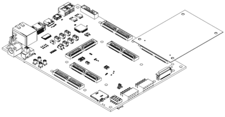
FPIC carrier and module Placement (PCB Edge)
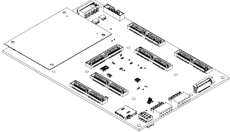
FPIC carrier and module Placement (Non- PCB Edge)
7.2.Module and Carrier Alignment
The FPIC module connector must align correctly with the corresponding carrier connector. Ensure proper connector orientation and engagement, following the pin numbering and mechanical drawings provided in this manual.

8.FPIC Pinouts
The FPIC connector provides 80 positions for user I/O, power supplies, high-speed transceiver signals, reference clocks, and module-management signals. The pin assignments vary depending on the selected FPIC variant.
Refer to the corresponding pinout diagram when designing or interfacing an FPIC module with a carrier board. Ensure that all signals are connected according to the requirements of the selected variant.
8.1.FPIC-ST Connector Pinout
The FPIC-ST connector provides 24 differential user I/O pairs, eight clock-capable I/O pairs, power and ground connections, and module-management signals. It does not support dedicated GT transceiver lanes.
| Pin Description | Pin Number | Pin Number | Pin Description |
|---|---|---|---|
| 5V | 1 | 2 | PG_M2C/PRSNT_M2C |
| GND | 3 | 4 | GND |
| IO0_P/CLK0_P | 5 | 6 | IO1_P/CLK1_P |
| IO0_N/CLK0_N | 7 | 8 | IO1_N/CLK1_N |
| IO2_P | 9 | 10 | IO3_P |
| IO2_N | 11 | 12 | IO3_N |
| GND | 13 | 14 | GND |
| IO4_P | 15 | 16 | IO5_P |
| IO4_N | 17 | 18 | IO5_N |
| IO6_P | 19 | 20 | IO7_P |
| IO6_N | 21 | 22 | IO7_N |
| GND | 23 | 24 | GND |
| IO8_P/CLK2_P | 25 | 26 | IO9_P/CLK3_P |
| IO8_N/CLK2_N | 27 | 28 | IO9_N/CLK3_N |
| IO10_P | 29 | 30 | IO11_P |
| IO10_N | 31 | 32 | IO11_N |
| GND | 33 | 34 | GND |
| IO12_P/CLK4_P | 35 | 36 | IO13_P/CLK5_P |
| IO12_N/CLK4_N | 37 | 38 | IO13_N/CLK5_N |
| IO14_P | 39 | 40 | IO15_P |
| IO14_N | 41 | 42 | IO15_N |
| GND | 43 | 44 | GND |
| IO16_P | 45 | 46 | IO17_P |
| IO16_N | 47 | 48 | IO17_N |
| IO18_P | 49 | 50 | IO19_P |
| IO18_N | 51 | 52 | IO19_N |
| GND | 53 | 54 | GND |
| IO20_P/CLK6_P | 55 | 56 | IO21_P/CLK7_P |
| IO20_N/CLK6_N | 57 | 58 | IO21_N/CLK7_N |
| IO22_P | 59 | 60 | IO23_P |
| IO22_N | 61 | 62 | IO23_N |
| GND | 63 | 64 | GND |
| RES | 65 | 66 | RES |
| RES | 67 | 68 | RES |
| GA0 | 69 | 70 | GA1 |
| VIO1 | 71 | 72 | SCL |
| VIO2 | 73 | 74 | SDA |
| GND | 75 | 76 | GND |
| 3.3V | 77 | 78 | 3.3V |
| 3.3V | 79 | 80 | 3.3V |
8.2.FPIC-GT4 Connector Pinout
The FPIC-GT4 connector provides 4 GT transceiver lanes (GT Quad 0, lanes 0–3), one reference clock pair (REF_CLK0), 16 IO differential pairs, and management signals. Pins 18–36 (even) and 21–35 (odd) are NC and reserved for GT8 use — they SHALL NOT be connected on GT4 modules.
| Pin Description | Pin Number | Pin Number | Pin Description |
|---|---|---|---|
| GT_TX0_P | 1 | 2 | GT_RX0_P |
| GT_TX0_N | 3 | 4 | GT_RX0_N |
| GT_TX1_P | 5 | 6 | GT_RX1_P |
| GT_TX1_N | 7 | 8 | GT_RX1_N |
| GT_TX2_P | 9 | 10 | GT_RX2_P |
| GT_TX2_N | 11 | 12 | GT_RX2_N |
| GT_TX3_P | 13 | 14 | GT_RX3_P |
| GT_TX3_N | 15 | 16 | GT_RX3_N |
| REF_CLK0_P | 17 | 18 | NC |
| REF_CLK0_N | 19 | 20 | NC |
| NC | 21 | 22 | NC |
| NC | 23 | 24 | NC |
| NC | 25 | 26 | NC |
| NC | 27 | 28 | NC |
| NC | 29 | 30 | NC |
| NC | 31 | 32 | NC |
| NC | 33 | 34 | NC |
| NC | 35 | 36 | NC |
| IO0_P/CLK0_P | 37 | 38 | IO1_P/CLK1_P |
| IO0_N/CLK0_N | 39 | 40 | IO1_N/CLK1_N |
| IO2_P | 41 | 42 | IO3_P |
| IO2_N | 43 | 44 | IO3_N |
| IO4_P | 45 | 46 | IO5_P |
| IO4_N | 47 | 48 | IO5_N |
| IO6_P | 49 | 50 | IO7_P |
| IO6_N | 51 | 52 | IO7_N |
| IO8_P/CLK2_P | 53 | 54 | IO9_P/CLK3_P |
| IO8_N/CLK2_N | 55 | 56 | IO9_N/CLK3_N |
| IO10_P | 57 | 58 | IO11_P |
| IO10_N | 59 | 60 | IO11_N |
| IO12_P | 61 | 62 | IO13_P |
| IO12_N | 63 | 64 | IO13_N |
| IO14_P | 65 | 66 | IO15_P |
| IO14_N | 67 | 68 | IO15_N |
| RES | 69 | 70 | GA0 |
| PG_M2C/ PRSNT_M2C | 71 | 72 | GA1 |
| VIO1 | 73 | 74 | SCL |
| VIO2 | 75 | 76 | SDA |
| 5V | 77 | 78 | 3.3V |
| 5V | 79 | 80 | 3.3V |
8.3.FPIC-GT8 Connector Pinout
The FPIC-GT8 connector provides 8 GT transceiver lanes across two quads (Quad 0: lanes 0–3, Quad 1: lanes 4–7), two independent reference clock pairs (REF_CLK0 for Quad 0, REF_CLK1 for Quad 1), 16 IO differential pairs, and management signals.
| Pin Description | Pin Number | Pin Number | Pin Description |
|---|---|---|---|
| GT_TX0_P | 1 | 2 | GT_RX0_P |
| GT_TX0_N | 3 | 4 | GT_RX0_N |
| GT_TX1_P | 5 | 6 | GT_RX1_P |
| GT_TX1_N | 7 | 8 | GT_RX1_N |
| GT_TX2_P | 9 | 10 | GT_RX2_P |
| GT_TX2_N | 11 | 12 | GT_RX2_N |
| GT_TX3_P | 13 | 14 | GT_RX3_P |
| GT_TX3_N | 15 | 16 | GT_RX3_N |
| REF_CLK0_P | 17 | 18 | REF_CLK1_P |
| REF_CLK0_N | 19 | 20 | REF_CLK1_N |
| GT_TX4_P | 21 | 22 | GT_RX4_P |
| GT_TX4_N | 23 | 24 | GT_RX4_N |
| GT_TX5_P | 25 | 26 | GT_RX5_P |
| GT_TX5_N | 27 | 28 | GT_RX5_N |
| GT_TX6_P | 29 | 30 | GT_RX6_P |
| GT_TX6_N | 31 | 32 | GT_RX6_N |
| GT_TX7_P | 33 | 34 | GT_RX7_P |
| GT_TX7_N | 35 | 36 | GT_RX7_N |
| IO0_P/CLK0_P | 37 | 38 | IO1_P/CLK1_P |
| IO0_N/CLK0_N | 39 | 40 | IO1_N/CLK1_N |
| IO2_P | 41 | 42 | IO3_P |
| IO2_N | 43 | 44 | IO3_N |
| IO4_P | 45 | 46 | IO5_P |
| IO4_N | 47 | 48 | IO5_N |
| IO6_P | 49 | 50 | IO7_P |
| IO6_N | 51 | 52 | IO7_N |
| IO8_P/CLK2_P | 53 | 54 | IO9_P/CLK3_P |
| IO8_N/CLK2_N | 55 | 56 | IO9_N/CLK3_N |
| IO10_P | 57 | 58 | IO11_P |
| IO10_N | 59 | 60 | IO11_N |
| IO12_P | 61 | 62 | IO13_P |
| IO12_N | 63 | 64 | IO13_N |
| IO14_P | 65 | 66 | IO15_P |
| IO14_N | 67 | 68 | IO15_N |
| RES | 69 | 70 | GA0 |
| PG_M2C/ PRSNT_M2C | 71 | 72 | GA1 |
| VIO1 | 73 | 74 | SCL |
| VIO2 | 75 | 76 | SDA |
| 5V | 77 | 78 | 3.3V |
| 5V | 79 | 80 | 3.3V |
9.FPIC User I/O Pins
The FPIC interface includes user-defined I/O pins that may operate as single-ended signals or differential pairs. I/O pin voltage levels are determined by the VIO rail.
| Parameter | Specification | Notes |
|---|---|---|
| Supported voltage range (VIO) | 1.2 V to 3.3V | Set by carrier |
| Signal tolerance | VIO ± 200 mV | Neither side SHALL exceed this |
| Differential impedance | 100? ± 10% | For LVDS operation |
| I/O standards supported | LVCMOS, LVTTL, SSTL, HSTL, LVDS | FPGA bank dependent |
| ST-FPIC IO count | 48 SE / 24 differential pairs | IO0IO23 |
| GT-FPIC IO count | 32 SE / 16 differential pairs | IO0IO15 |
10.FPIC Pin Definitions
10.1.FPIC ST Pin Definition
10.1.1.User I/O Signals
10.1.2.I/O Bank Assignment Recommendation
To ensure compatibility across FPGA families and to preserve the clock-capable I/O relationships, the FPIC-ST user I/O signals should be assigned to FPGA I/O banks as follows:
-
The IO0_P/N through IO11_P/N differential pairs should be routed to a single FPGA I/O bank. (BANK A)
-
The IO12_P/N through IO23_P/N differential pairs should be routed to a second FPGA I/O bank. (BANK B)
-
FPGA devices that provide a single I/O bank with sufficient user I/O resources may route IO0_P/N through IO23_P/N to the same FPGA I/O bank.
- Partial assignment of the IO12–IO23 group before completing the IO0–IO11 group, or intermixing signals between the two FPGA I/O banks, SHALL NOT be permitted.
10.1.3.Clock-Capable I/O Signals and Associated I/O Signals
Clock-capable IO pairs are physically routed to FPGA global or regional clock-capable inputs. They support reference clocks, source-synchronous interfaces, and timing-critical signals.
| Variant | Mandatory CLK pairs | Optional CLK pairs | Total |
|---|---|---|---|
| FPIC-ST | CLK0, CLK1, CLK4, CLK5 | CLK2, CLK3, CLK6, CLK7 | 8 |
Recommended Clock-Capable I/O Signal Association:
| Primary CC Signal | Preferred User I/O Signals | Secondary CC Signal |
|---|---|---|
| IO0_P/N | IO1 - IO11 | IO1_P/N |
| IO12_P/N | IO12 - IO23 | IO13_P/N |
Recommendation: For carrier board designs using UltraScale or UltraScale+ FPGAs, where available, it is recommended to assign the GC_QBC – capable pins to IO0_P/CLK0_P and IO0_N/CLK0_N to support clock-related functionality. This recommendation is optional.
10.1.4.Power rails
-
5V – Main power supply provided by the carrier to the FPIC-GT module, supporting up to 2 A per connector pin.
-
3V – Auxiliary 3.3V power supplied by the carrier for module circuitry, supporting up to 2 A per connector pin.
-
GND – Common ground reference shared between the carrier and the module.
10.1.5.VIO Reference Voltages
The VIO1 and VIO2 signals define the reference I/O bank voltage supplied by the carrier to the FPIC-ST module. These voltages determine the operating voltage of the associated user I/O signals and shall be compatible with the I/O standards supported by both the FPGA and the module.
NOTE:
If all 24 differential I/O pairs (IO0–IO23) are implemented within a single FPGA I/O bank, either VIO1 or VIO2 may be connected, provided the selected supply voltage matches the FPGA I/O bank reference voltage
10.2.FPIC-GT4 / GT8 Pin Definitions
10.2.1.High-Speed Transceiver Signals
GT_TX[0..7]_P, GT_TX[0..7]_N – Differential high-speed transmitter pairs from the FPGA to the FPIC-GT connector. These signals are intended for high-speed serial interfaces such as Ex: PCI Express, Ethernet, JESD204, Aurora and other FPGA transceiver-based protocols.
GT_RX[0..7]_P, GT_RX[0..7]_N – Differential high-speed receiver pairs from the FPIC-GT connector to the FPGA. These signals shall be routed as controlled-impedance differential pairs in accordance with the Peripheral design guidelines.
REF_CLK0_P/N – Differential reference clock pair associated with GT Quad 0.
REF_CLK1_P/N – Differential reference clock pair associated with GT Quad 1.
The reference clock pairs provide low-jitter clock sources for the FPGA transceiver quads and should be connected to dedicated transceiver reference clock inputs.
Note:
The FPIC-GT8 connector provides eight transmit and eight receive differential transceiver pairs. The FPIC-GT4 connector provides only GT Quad 0. The signals corresponding to GT Quad 1, including REF_CLK1, are not connected in the FPIC-GT4 connector.
10.2.2.I/O Bank Assignment Recommendation
-
The IO0_P/N through IO7_P/N differential pairs should be routed to a single FPGA I/O bank.
-
The IO8_P/N through IO15_P/N differential pairs should be routed to a second FPGA I/O bank.
-
FPGA devices that provide a single I/O bank with sufficient user I/O resources may route IO0_P/N through IO15_P/N to the same FPGA I/O bank.
-
Partial assignment of the IO8–IO15 group before completing the IO0–IO7 group, or intermixing signals between the two FPGA I/O banks, SHALL NOT be permitted.
10.2.3.Clock-Capable I/O Signals and Associated I/O Signals
Clock-capable IO pairs are physically routed to FPGA global or regional clock-capable inputs. They support reference clocks, source-synchronous interfaces, and timing-critical signals.
| Variant | Mandatory CLK pairs | Optional CLK pairs | Total |
|---|---|---|---|
| FPIC-GT4 | CLK0, CLK1, CLK2, CLK3 | - | 4 (all mandatory) |
| FPIC-GT8 | CLK0, CLK1, CLK2, CLK3 | - | 4 (all mandatory) |
Recommended Clock-Capable I/O Signal Association:
| Primary CC Signal | Preferred User I/O Signals | Secondary CC Signal |
|---|---|---|
| IO0_P/N | IO1 IO7 | IO1_P/N |
| IO8_P/N | IO8 IO15 | IO9_P/N |
10.2.4.GT Transceiver Data Pins
GT transceiver pins carry high-speed serial data between the module and carrier FPGA SERDES resources. They SHALL NOT be repurposed as GPIO or used for low-speed logic.
| Parameter | Specification |
|---|---|
| Lane direction - TX | GT_TXx_P/N: carrier ? module (carrier drives) |
| Lane direction - RX | GT_RXx_P/N: module ? carrier (module drives) |
| Differential impedance | 100? ± 10% end-to-end |
| P/N polarity | SHALL be preserved. Inversion only if compensated in FPGA SERDES |
| AC coupling | 100nF 0402 SHALL be placed on TX pairs within 5mm of connector |
| Unused lanes | SHALL be SERDES-terminated or powered down. SHALL NOT float |
| Supported transceivers | GTR, GTH, GTX, GTY (Xilinx/AMD); GX, GT (Intel/Altera) |
10.2.5.Reference Clock Pins (REF_CLK0, REF_CLK1)
Reference clock pairs supply the timing reference for FPGA SERDES quads. REF_CLK0 serves GT Quad 0 (lanes 0–3). REF_CLK1 serves GT Quad 1 (lanes 4–7) and is available on FPIC-GT8 only.
| Parameter | Specification |
|---|---|
| Direction | Module ? carrier (module oscillator drives FPGA REFCLK input) |
| Oscillator location | SHALL reside on the FPIC module |
| Impedance | 100? ± 10% differential |
| Polarity | SHALL be preserved (P/N) |
| Unused REF_CLK pairs | SHALL remain electrically safe no floating differential pairs |
| Repurposing | REF_CLK pins SHALL NOT be used for user I/O or low-speed signals |
10.2.6.Power rails
-
5V – Main power supply provided by the carrier to the FPIC-GT module, supporting up to 2 A per connector pin.
-
3V – Auxiliary 3.3V power supplied by the carrier for module circuitry, supporting up to 2 A per connector pin.
-
GND – Common ground reference shared between the carrier and the module.
10.2.7.VIO Reference Voltages
The VIO1 and VIO2 signals define the reference I/O bank voltage supplied by the carrier to the FPIC-GT module. These voltages determine the operating voltage of the associated user I/O signals and shall be compatible with the I/O standards supported by both the FPGA and the module.
VIO1 – Reference I/O bank voltage associated with the IO0_P/N through IO7_P/N differential I/O group.
VIO2 – Reference I/O bank voltage associated with the IO8_P/N through IO15_P/N differential I/O group.
NOTE:
If all 16 differential I/O pairs are assigned to a single FPGA I/O bank, VIO1 and VIO2 shall be connected to the same I/O bank supply voltage to maintain a common reference voltage for all user I/O signals.
10.3.PG_M2C/PRSNT_M2C
The PG_M2C / PRSNT_M2C signal indicates module presence and power-good status. The carrier shall provide a 10 kΩ ±10% pull-down resistor, while the module shall provide a 1 kΩ ±10% pull-up resistor to 3.3 V. Once all required power rails are stable, the module shall drive this signal High to indicate power-good status.
10.4.Geographic Address Pins (GA0, GA1)
GA pins identify the physical slot position of the installed FPIC module and determine the module’s I2C address.
| GA1 | GA0 | Slot / Port ID | I2C EEPROM Address |
|---|---|---|---|
| 0 | 0 | Slot 0 | 0x50 |
| 0 | 1 | Slot 1 | 0x51 |
| 1 | 0 | Slot 2 | 0x52 |
| 1 | 1 | Slot 3 | 0x53 |
Note:
The carrier SHALL pull GA0 and GA1 to defined logic levels before module power-up. GA pins SHALL NOT float.
10.5.SCL / SDA — I2C Management
| Parameter | Specification |
|---|---|
| Pull-up resistors | 4.7k on the carrier side (SHALL NOT be placed on module) |
| I/O voltage domain | Fixed 3.3V on carrier |
| Voltage tolerance | 3.3V ± 300mV |
| Minimum speed | Standard-mode 100kHz |
| Recommended speed | Fast mode 400kHz |
| SDA function | Bidirectional data line |
| SCL function | Clock line (carrier is master) |
11.FPIC Module Management - EEPROM & I2C
11.1.EEPROM Requirements
Every FPIC module SHALL contain a non-volatile EEPROM accessible via the I2C bus on SDA/SCL. The EEPROM SHALL store module identification and power configuration data in the format defined below.
Recommended EEPROM: Microchip 24AA025E48 or 24AA025E64 in the SOIC package. The A2 address pin shall be connected to Logic 0 (GND).
11.2.FPIC Module I2C Address Assignment
The FPIC module EEPROM SHALL respond at a 7-bit I2C address determined by the GA0 and GA1 pins as follows:
Address = 0b1010_0_GA1_GA0
Range: 0x50 (Slot 0) to 0x53 (Slot 3)
12.FPIC Compatibility Matrix
The following matrix defines the compatibility between FPIC module and carrier variants. All FPIC variants use the same PCB outline (58.00mm × 80.00mm) and mounting hole pattern.
Module \ Carrier FPIC-ST Carrier FPIC-GT4 Carrier FPIC-GT8 Carrier
FPIC-ST Module ✓ Full - all IO and power signals functional ✗ Incompatible ✗ Incompatible
FPIC-GT4 Module ✗ Incompatible ✓ Full - lanes 0-3 and REF_CLK0 fully functional ✓ Partial - lanes 0-3 and REF_CLK0 functional; lanes 4-7 NC on module
FPIC-GT8 Module ✗ Incompatible ✓ Partial - lanes 0-3 active; lanes 4-7 must be powered down in FPGA ✓ Full - all 8 lanes and both REF_CLKs functional
13.FPIC Identification and Marking
All modules and carrier boards claiming compliance with the FPIC Specification SHALL implement the FPIC identification marking in accordance with the following requirements.
| Parameter | Requirement |
|---|---|
| Marking | The appropriate FPIC designation (FPIC-ST, FPIC-GT4, or FPIC-GT8) SHALL be displayed on both the FPIC module and the carrier board. |
| Compliance | Displaying the FPIC designation is mandatory for all products claiming compliance with the FPIC Specification. |
| Location | The FPIC designation SHALL be placed on the Left-hand side of the FPIC connector, as shown in the mechanical drawings. The text orientation shall be parallel to the connector. |
| Font | Montserrat Bold |
| Text Height | 2.54mm |
| Colour / Finish | The FPIC designation SHALL be implemented using an Overlay. |
| Connector Designator | The primary FPIC connector SHALL use the reference designator P1. Additional FPIC connectors, if present, SHALL be designated sequentially as P2, P3, etc. |
| Connector Pin Numbering | The connector pin numbers SHALL be identified on the PCB adjacent to the connector, as illustrated in the image below. Pin numbering SHALL clearly indicate the first and last pin locations and maintain the numbering sequence defined by the FPIC connector specification to ensure correct module orientation and assembly. |
| Visibility | The FPIC designation SHALL remain unobstructed by components, heatsinks, labels, or other mechanical features to ensure clear identification. |
| FPIC Connector Identification | For carrier boards implementing a single FPIC connector, the PCB overlay SHALL identify the connector as "FPIC-ST" or "FPIC-GT4 / FPIC-GT8", as applicable. For carrier boards implementing multiple FPIC connectors of the same or different standards, each connector SHALL be assigned a unique identifier A, B, C, or D. The PCB overlay SHALL display the identification in the format "FPIC |

FPIC Logo
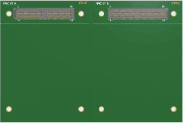
FPIC Carrier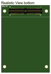
FPIC Module
Note: The placement, orientation, and dimensions of the FPIC designation shall conform to the mechanical drawings provided in this specification to ensure a consistent appearance across all FPIC-compliant modules and carrier boards.
14.Licensing
© 2026 Numato Systems Pvt Ltd. All rights reserved.
This specification — the FPIC (FPGA Peripheral Interface Connector) Standard — is licensed under the Creative Commons Attribution 4.0 International Licence (CC BY 4.0). You are free to implement, share, adapt, and build upon this standard for any purpose, including commercial use, provided that appropriate credit is given to Numato Systems Pvt Ltd as the originating author of the FPIC Standard.
FPIC name and designations: The FPIC name and the interface designations FPIC-ST, FPIC-GT4, and FPIC-GT8 are trademarks of Numato Systems Pvt Ltd. Use of these designations on products claiming FPIC compliance is permitted under the attribution terms above, provided the product fully conforms to the latest published version of this specification.
Compliance: Products displaying the FPIC designation SHALL fully conform to all mandatory (SHALL) requirements defined in this specification. Partial implementations SHALL NOT display the FPIC designation without clearly stating which variant (FPIC-ST, FPIC-GT4, FPIC-GT8) is supported and which requirements are not met.
Licence text: https://creativecommons.org/licenses/by/4.0/